

A kind of on-chip self-test circuit and method of storage unit for RRAM
A cell and self-test technology, applied to the on-chip self-test circuit and field of memory cells used in RRAM, can solve the problems of time-consuming and complicated test excitation, save array read operations, save test costs, and simplify The effect of the test sequence
- Summary
- Abstract
- Description
- Claims
- Application Information
AI Technical Summary
Problems solved by technology
Method used
Image

Examples
Embodiment Construction
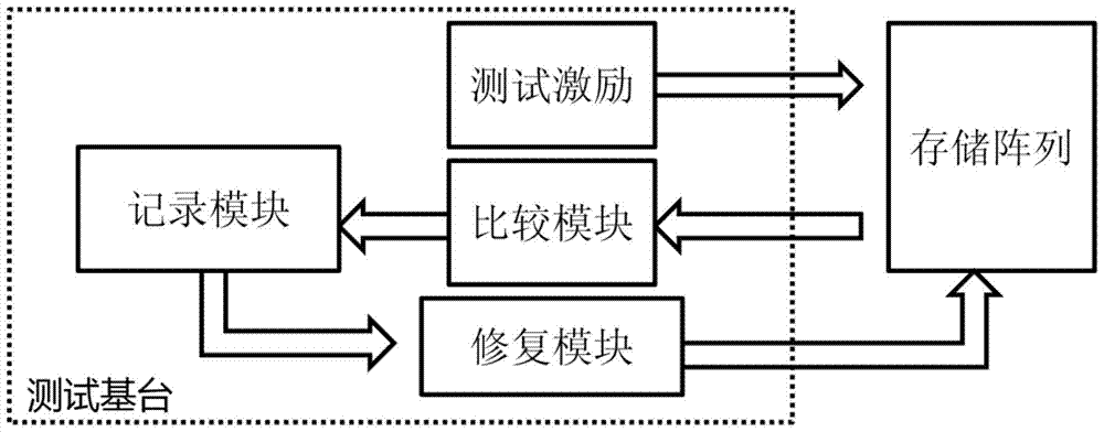
[0053] In view of this situation, the present invention is based on the basic structure and the basic operation process of the RRAM internal circuit, adding the latching mechanism of the successful flag bit that returns when writing verification at every turn, specifically as follows:
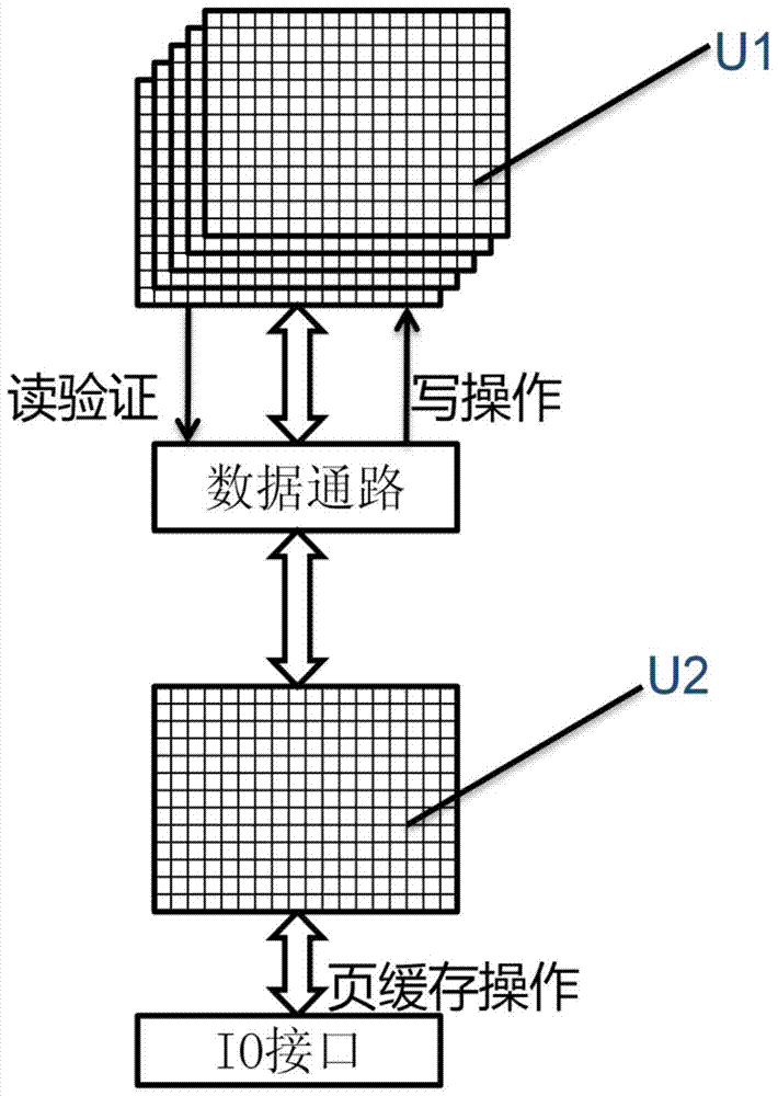
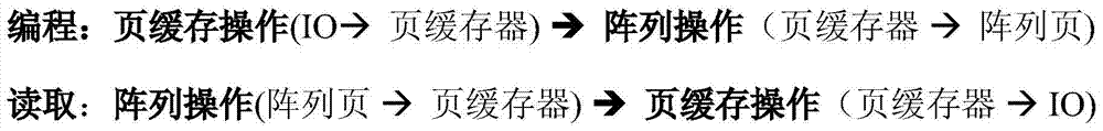
[0054] like Figure 4a , Figure 4b It is a schematic diagram of the implementation of the specific module of the present invention, and a latch mechanism is added between the data path and the page buffer, so as to complete the judgment function of the read verification result flag and the realization of the latch and write page buffer function, mainly including A control judgment logic module, a latch enabling module, a write-back address module, a latch module and a page buffer write-back module.
[0055] At the same time, the latch enable module and the write-back address module are added. If the read verification result of the current address is successful, the latch enable module will di...
PUM
 Abstract
Description
Claims
Application Information