A high-temperature oxidation-resistant readout circuit lead-out electrode and its preparation method
A technology that resists high temperature oxidation and reads out circuits, and is used in circuits, electrical components, and final product manufacturing.
- Summary
- Abstract
- Description
- Claims
- Application Information
AI Technical Summary
Problems solved by technology
Method used
Image
Examples
Embodiment 1
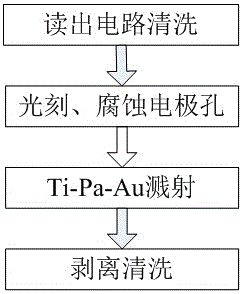
[0030] like figure 1 As shown, a preparation method of a high-temperature oxidation-resistant readout circuit lead-out electrode comprises the following steps:
[0031] Step a, readout circuit cleaning: if figure 2 As shown, after the readout circuit 1 is taped out from a silicon factory, the lead-out electrode is an Al metal layer 2 . The readout circuit 1 is used as the substrate, and it is firstly cleaned: each is washed three times with toluene, acetone, and ethanol in sequence, and the residual solution is blown dry with a nitrogen gun.
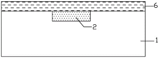
[0032] Step b, photolithography and etching electrode holes: on the readout circuit 1, apply photoresist AZ6130 at a speed of 3500 rpm for 30 seconds, the thickness of the coating is 2 μm, and the coating time is 30 seconds, and then at 80 ° C Pre-bake for 2 minutes to form a photoresist layer 6, such as image 3 shown. Use a photolithography machine to expose, use AZ300MIF developer to develop, and control the development time, so...
Embodiment 2
[0037] like figure 1 As shown, a preparation method of a high-temperature oxidation-resistant readout circuit lead-out electrode comprises the following steps:
[0038] Step a, readout circuit cleaning: if figure 2 As shown, after the readout circuit 1 is taped out from a silicon factory, the lead-out electrode is an Al metal layer 2 . The readout circuit 1 is used as the substrate, and it is firstly cleaned: each is washed three times with toluene, acetone, and ethanol in sequence, and the residual solution is blown dry with a nitrogen gun.
[0039] Step b, photolithography and etching electrode holes: on the readout circuit 1, apply photoresist AZ6130 for 30 seconds at a speed of 2500 rpm, with a coating thickness of 3 μm, and then pre-bake at 80°C for 3 minutes to form photoresist layer 6, such as image 3 shown. Use a photolithography machine to expose, use AZ300MIF developer to develop, and control the development time, so that the photoresist in the electrode hole ...
Embodiment 3
[0044] like figure 1 As shown, a preparation method of a high-temperature oxidation-resistant readout circuit lead-out electrode comprises the following steps:
[0045] Step a, readout circuit cleaning: if figure 2 As shown, after the readout circuit 1 is taped out from a silicon factory, the lead-out electrode is an Al metal layer 2 . The readout circuit 1 is used as the substrate, and it is firstly cleaned: each is washed three times with toluene, acetone, and ethanol in sequence, and the residual solution is blown dry with a nitrogen gun.
[0046] Step b, photolithography and etching electrode holes: on the readout circuit 1, apply photoresist AZ6130 at a speed of 2800 rpm for 30 seconds, with a coating thickness of 2.5 μm, and then pre-bake at 80°C for 2.5 minutes, Form a photoresist layer 6, such as image 3 shown. Use a photolithography machine to expose, use AZ300MIF developer to develop, and control the development time, so that the photoresist in the electrode h...
PUM
 Abstract
Description
Claims
Application Information


