Conversion card for testing probe card

A technology for testing probes and conversion cards, applied in the field of conversion cards, can solve the problems of cost, time, and cost increase.

Inactive Publication Date: 2015-11-25
詹定叡
View PDF9 Cites 3 Cited by
  • Summary
  • Abstract
  • Description
  • Claims
  • Application Information

AI Technical Summary

Problems solved by technology

[0002] For a long time, the semiconductor industry will first verify whether the DC probe card (ProbeCard) is available during the wafer reliability test (wafer acceptance test), because the DC probe card is responsible for the final stage of the test, before the IC is cut (WS: WaferSort ), the important role of whether the functional test is normal. When the IC test can work normally, the IC will be cut and packaged (FT: FinalTest; IChasbeenpackaged) and then followed by the classification (BIN) test. It can be seen that when the DC probe When the error rate of the card is high, it will directly affect the speed and quality of the subsequent shipments. However, as the IC function becomes stronger and stronger, the number of pins of the DC probe card increases, even as high as tens of thousands of pins. It costs tens of millions. If the DC probe card is judged to have a high error rate, it is necessary to clear the needle or even replace the card. These actions are very costly and time-consuming. Fabs and test factories often rush to deliver goods to customers. Often the card is replaced directly until the test is correct, and the cost of these replaced DC probe cards is directly absorbed by the fab and the test factory, so the inventory rate of DC probe cards often reaches several thousand Taiwan dollars Tens of thousands to hundreds of millions of grades, resulting in a substantial increase in costs

Method used


Image

  • Conversion card for testing probe card
  • Conversion card for testing probe card
  • Conversion card for testing probe card

Examples


Embodiment Construction

[0044] In order to further explain the technical solution of the present invention, the present invention will be described in detail below through specific examples.

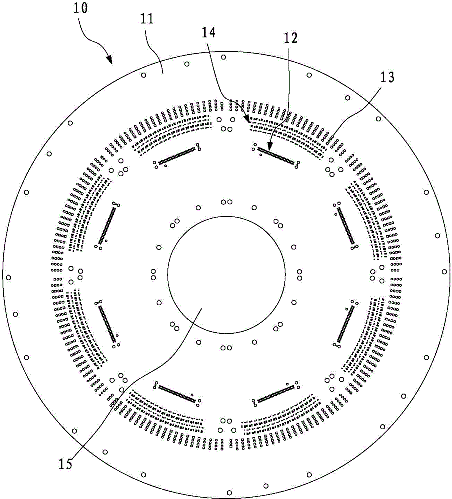
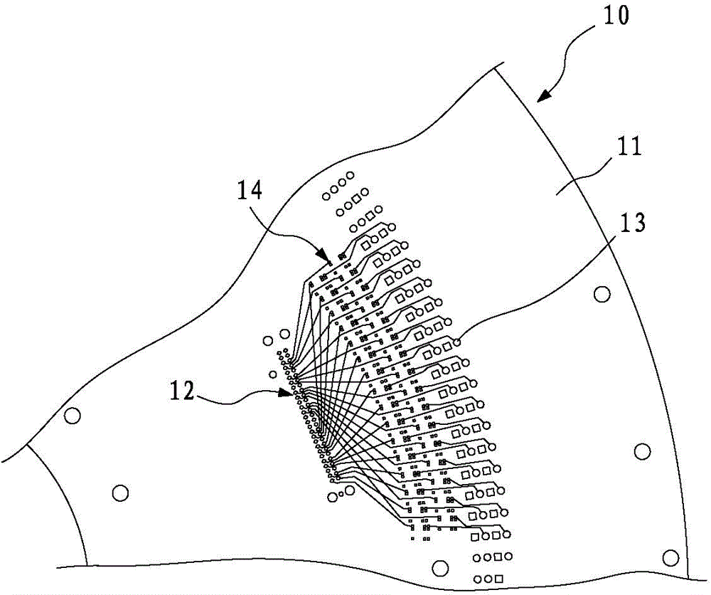
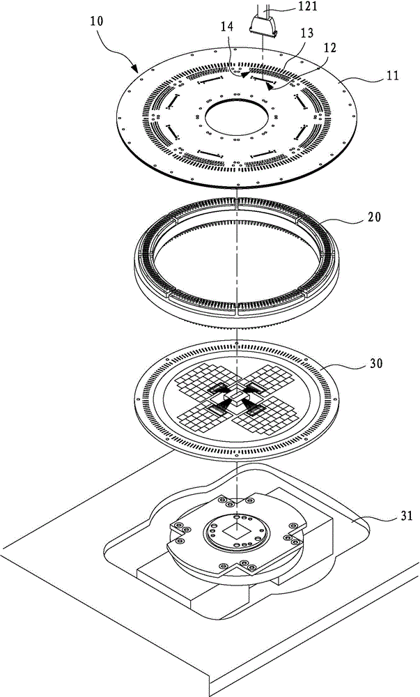
[0045] see Figure 1 to Figure 16 As shown, the structure of the conversion card 10 used to test the probe card (ProbeCard) of the present invention includes a board body 11, a first transmission unit 12, a second transmission unit 13 and a DC / AC conversion circuit 14, wherein:

[0046] In one embodiment, the plate body 11 has a perforation 15 for reducing weight, saving material, and further reducing manufacturing cost.

[0047] The first transmission unit 12 is arranged on the board body 11. The first transmission unit 12 is used to electrically connect to a predetermined test instrument to transmit AC signals. In this embodiment, the first transmission unit 12 can be electrically connected to the connection line 121 of the test instrument. The first transmission unit 12 is evenly arranged on the board body ...


PUM


Abstract

Provided is a conversion card for testing a probe card. The conversion card comprises a plate body, and a plurality of first transmission units, a plurality of second transmission units and a DC / AC conversion circuit; and the first transmission units, the second transmission units and the DC / AC conversion circuit are disposed on the plate body. The first transmission units are electrically connected with a test instrument. The second transmission units are electrically connected with interfaces of the probe card. The DC / AC converting circuit is electrically connected with the first transmission units and the second transmission units. AC signals are transmitted by the first transmission units, and the AC signals are transmitted to the DC probe card through the DC / AC conversion circuit, the second transmission units and the interfaces of the probe card. By using principles of an AC circuit and a transmission line, the conversion card cooperates with AC signal test instruments of a logic analyzer, an oscilloscope, a time-domain reflectometer, a frequency domain network analyzer, an error code generator, an eye pattern analyzer and the like. An AC method is used to perform error analysis and improvement on the DC probe card, thereby preventing the misjudging error rate of the probe card, reducing the card changing rate and the pin removing rate, and reducing the inventory ratio of the DC probe card.

Description

technical field [0001] The invention relates to a conversion card, in particular to a conversion card for testing probe cards. Background technique [0002] For a long time, the semiconductor industry will first verify whether the DC probe card (ProbeCard) is available during the wafer reliability test (wafer acceptance test), because the DC probe card is responsible for the final stage of the test, before the IC is cut (WS: WaferSort ), the important role of whether the functional test is normal. When the IC test can work normally, the IC will be cut and packaged (FT: FinalTest; IChasbeenpackaged) and then followed by the classification (BIN) test. It can be seen that when the DC probe When the error rate of the card is high, it will directly affect the speed and quality of the subsequent shipments. However, as the IC function becomes stronger and stronger, the number of pins of the DC probe card increases, even as high as tens of thousands of pins. It costs tens of millio...

Claims


Application Information

Patent Timeline
Patent Type & Authority Applications(China)
IPC IPC(8): G01R15/00G01R35/02
Inventor 詹定叡
Owner 詹定叡
Why Eureka
Try Eureka