Hole layer optical proximity correction method for avoiding large aspect ratio pattern

A technology of optical proximity correction and aspect ratio, which is applied in optical, patterned surface photoengraving process, and originals for opto-mechanical processing. , to achieve the effect of minimum edge position error

Active Publication Date: 2015-11-25
SEMICON MFG INT (SHANGHAI) CORP
View PDF5 Cites 13 Cited by
  • Summary
  • Abstract
  • Description
  • Claims
  • Application Information

AI Technical Summary

Problems solved by technology

But in dense spacing, there is not enough room to insert diffuser bars
Therefore, it cannot completely solve the problem
[0012] 2. Limit aspect ratio in OPC menu
[0013] This coercive approach will result in the preservation of edge position errors

Method used


Image

  • Hole layer optical proximity correction method for avoiding large aspect ratio pattern
  • Hole layer optical proximity correction method for avoiding large aspect ratio pattern
  • Hole layer optical proximity correction method for avoiding large aspect ratio pattern

Examples


Embodiment Construction

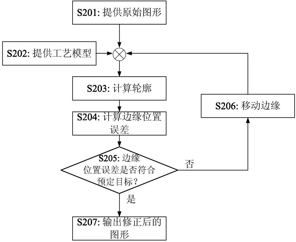
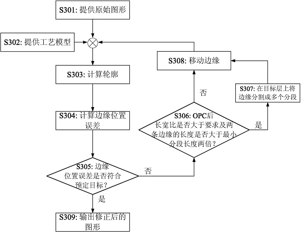
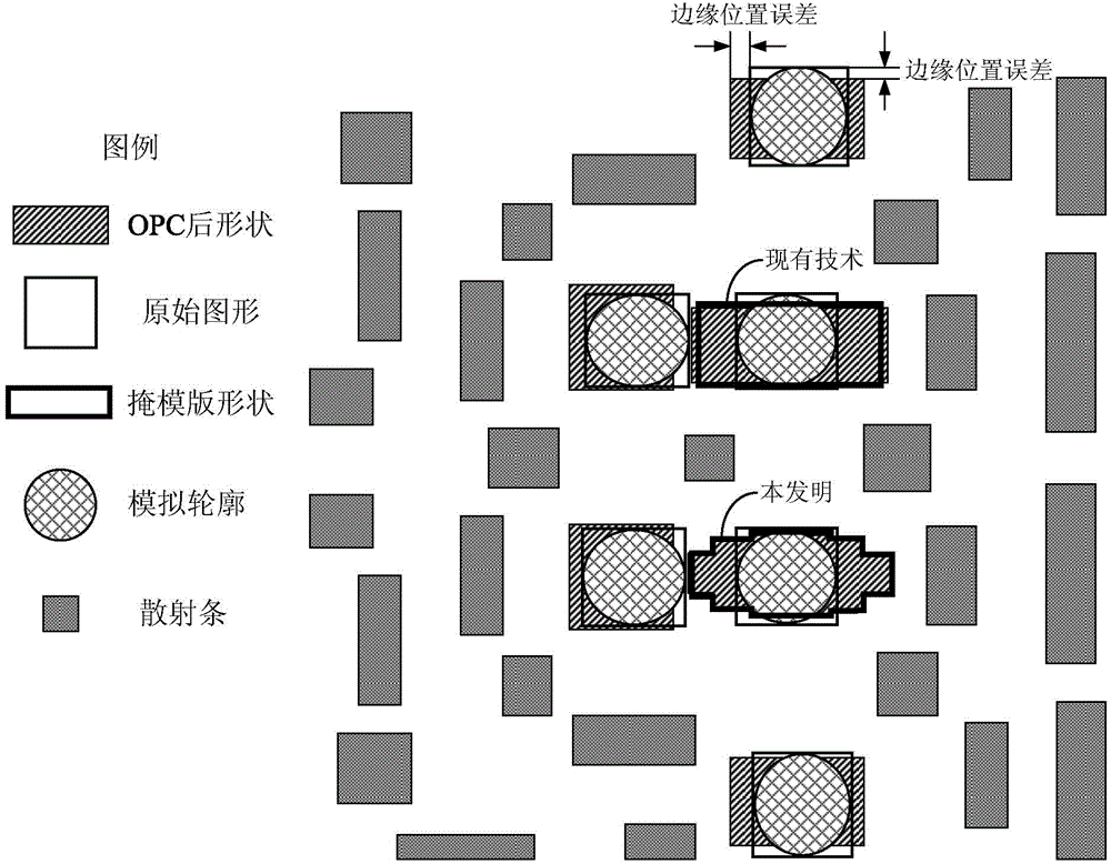
[0038] For comparison, before describing the hole layer optical proximity correction method for avoiding large aspect ratio patterns of the present invention, first describe how the traditional hole layer optical proximity correction method in the prior art is implemented. figure 1 It is a flow chart of a traditional optical proximity correction method for a hole layer in the prior art; image 3 It is a schematic diagram comparing the post-OPC shape and the shape of the reticle obtained by using the traditional hole layer optical proximity correction method and the hole layer optical proximity correction method avoiding large aspect ratio patterns according to an embodiment of the present invention. Such as figure 1 and combine image 3 As shown, the process includes steps:

[0039] Execute step S201 to provide the original graphics to be corrected;

[0040] Execute step S202 to provide an optical proximity correction process model (not shown), which is an OPC algorithm;

...


PUM


Abstract

The present invention provides a hole layer optical proximity correction method for avoiding large aspect ratio pattern. The hole layer optical proximity correction method comprises: A, providing an original pattern to be corrected; B, providing a process model of OPC; C, calculating the hole outline according to the original pattern or the post-OPC pattern and the process model; D, calculating the EPE of each edge of the post-OPC pattern; E, determining whether the EPE meets the predetermined target, if not, performing a step F, and if so, performing a step I; F, determining whether the aspect ratio after the OPC is larger than the requirement and the lengths of the two edges in the length direction and the width direction are larger than two times the minimum segment length in each pattern, if so, performing a step G and then performing a step H, and if not, directly performing the step H; G, cutting the edge into a plurality of segments on the target layer; H, moving the edge, and returning to the step C; and I, outputting the post-OPC pattern. According to the present invention, the good fidelity can be obtained during the mask plate manufacturing process, and the high precision at the OPC simulation stage can be ensured.

Description

technical field [0001] The present invention relates to the technical field of optical proximity correction in the semiconductor manufacturing process, in particular, the present invention relates to a method for avoiding large aspect ratio patterns in the optical proximity correction (Optical Proximity Correction, OPC) process of the hole layer. Background technique [0002] With the rapid development of integrated circuit design, how to reduce the deformation and deviation of layout patterns after lithography, suppress the negative effects of optical proximity effect, and improve the yield of chip production plays a key role in the development of chip manufacturing industry. To solve this problem, a method generally adopted in the industry is optical proximity correction, which reduces the deviation of the photolithography pattern obtained by exposure by changing the shape of the original layout pattern. [0003] In the prior art, the process of optical proximity correctio...

Claims


Application Information

Patent Timeline
Patent Type & Authority Applications(China)
IPC IPC(8): G03F1/36
Inventor 张婉娟
Owner SEMICON MFG INT (SHANGHAI) CORP
Why Eureka
Try Eureka