Mixed type three-dimensional on-chip network

A network-on-chip, hybrid technology, applied in the direction of instruments, electrical digital data processing, computers, etc., can solve the problems of increased communication power consumption, increased system transmission delay, etc., to improve internal bandwidth, shorten global interconnection length, increase The effect of interconnection

Active Publication Date: 2015-11-25
INSPUR BEIJING ELECTRONICS INFORMATION IND
View PDF4 Cites 5 Cited by
  • Summary
  • Abstract
  • Description
  • Claims
  • Application Information

AI Technical Summary

Problems solved by technology

The increase of the connection length directly brings about the increase of the system transmission delay, which limits the increase of the data transmission frequency. At the same time, due to the increase of the global connection length and the number of data forwarding times, the communication power consumption of the system will also increase.

Method used


Image

  • Mixed type three-dimensional on-chip network
  • Mixed type three-dimensional on-chip network
  • Mixed type three-dimensional on-chip network

Examples


Embodiment Construction

[0030] The following will clearly and completely describe the technical solutions in the embodiments of the present invention with reference to the accompanying drawings in the embodiments of the present invention. Obviously, the described embodiments are only some, not all, embodiments of the present invention. Based on the embodiments of the present invention, all other embodiments obtained by persons of ordinary skill in the art without creative efforts fall within the protection scope of the present invention.

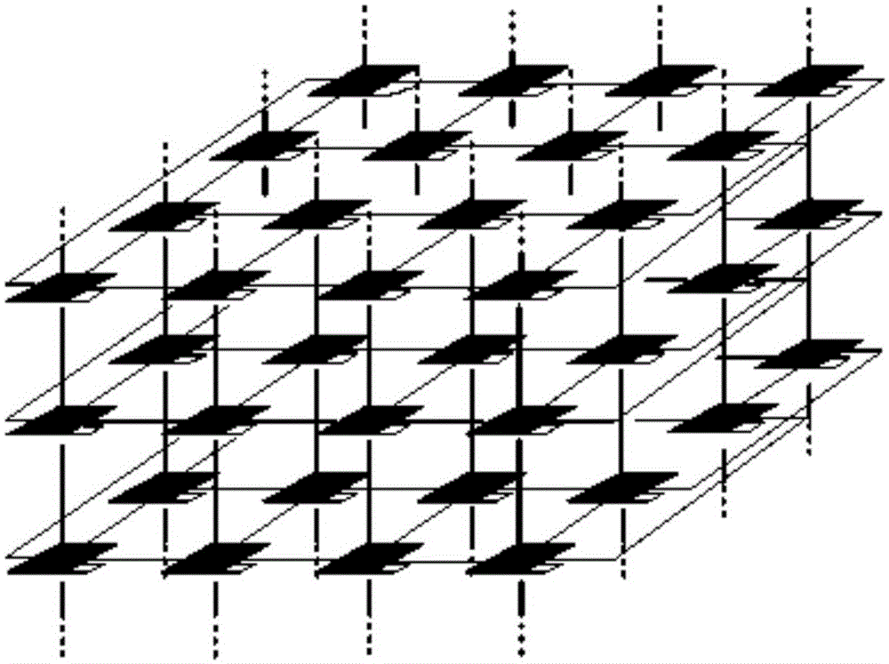
[0031] The embodiment of the invention discloses a hybrid three-dimensional on-chip network to reduce the length of the connection and the diameter of the network, reduce system transmission delay, and reduce communication power consumption.

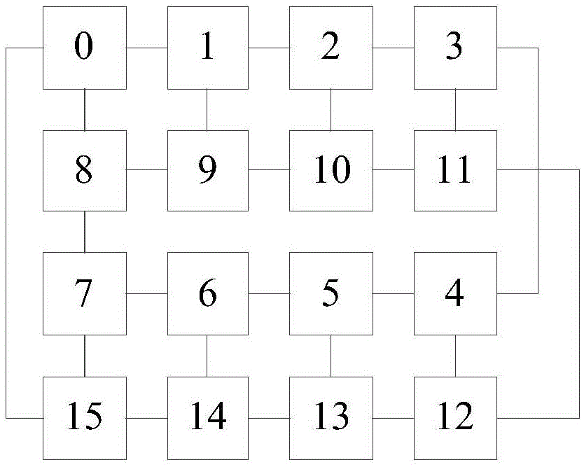
[0032] see figure 1 , a hybrid three-dimensional network on chip provided by an embodiment of the present invention, including:

[0033] A plurality of horizontal sublayers stacked in the vertical direction; wherein, the hor...


PUM


Abstract

The embodiment of the invention discloses a mixed type three-dimensional on-chip network. The mixed type three-dimensional on-chip network comprises a plurality of horizontal sub-layers which are stacked in the perpendicular direction, perpendicular buses and a perpendicular bus controller, wherein the same topological structure is kept for horizontal route units in all the horizontal sub-layers, the perpendicular buses are used for connecting the horizontal route units, located on the same vertical line, in the horizontal sub-layers, the number of the perpendicular buses corresponds to the number of the horizontal route units in the horizontal sub-layers, and the perpendicular bus controller is used for controlling the occupation right of the perpendicular buses. The horizontal sub-layers are stacked in the perpendicular direction to form the three-dimensional on-chip network, interconnection in the perpendicular direction is improved, the global interconnection length in a chip is shortened, the bandwidth in the chip is improved, and delay and power consumption of data transmission are reduced.

Description

technical field [0001] The present invention relates to the technical field of on-chip network, and more specifically, relates to a hybrid three-dimensional on-chip network. Background technique [0002] Network-on-Chip (NoC) interconnection structure has become the development trend of chip architecture design, and it is one of the effective solutions for future on-chip IP core interconnection. The multi-core processor system-on-a-chip based on the NoC architecture can realize the separation of computing and communication. The computing subsystem composed of IP cores can independently complete computing tasks, and the communication subsystem composed of NoC is responsible for high-speed data exchange between IP cores. As the integrated circuit process enters the 14nm process era, the design scale of NoC continues to expand. Since all resource nodes are laid out on the plane, and the layout and wiring are carried out on the two-dimensional plane, the interconnection lines be...

Claims


Application Information

Patent Timeline
IPC IPC(8): G06F15/173
Inventor 张闯
Owner INSPUR BEIJING ELECTRONICS INFORMATION IND
Why Eureka
Try Eureka