

Method of forming a transistor
A transistor and area technology, applied in semiconductor/solid-state device manufacturing, electrical components, circuits, etc., to achieve the effects of short etching time, improved performance, and easy control of the etching process
- Summary
- Abstract
- Description
- Claims
- Application Information
AI Technical Summary
Problems solved by technology
Method used
Image

Examples
Embodiment Construction
[0031] As mentioned in the background art, the performance of the transistors in the core region formed in the prior art needs to be further improved.
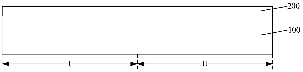
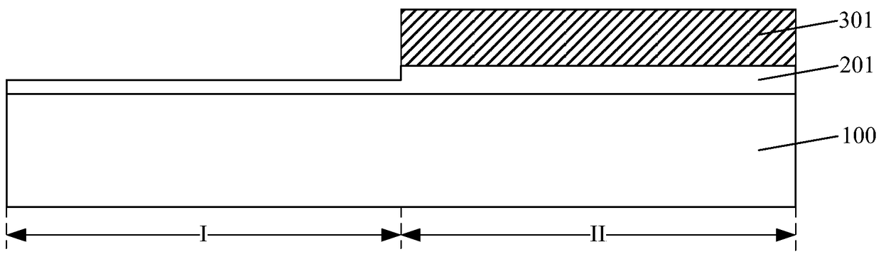
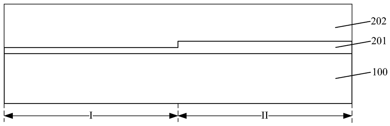
[0032] In the prior art, in the process of forming the transistors in the core area and the transistors in the input / input area, a dummy gate dielectric material layer covering both the core area and the input / output area is generally formed on the surface of the semiconductor substrate, and a layer of dummy gate material located in the dummy gate A dummy gate material layer on the surface of the dielectric layer; then the dummy gate dielectric material layer and the dummy gate material layer are patterned to form a dummy gate material layer on the core area and a dummy gate material layer on the surface of the dummy gate material layer dummy gate layer, and the gate dielectric layer located on the surface of the input / output area and the gate dielectric layer and the gate layer, so that the thickness of the dummy gate dielectr...
PUM
 Abstract
Description
Claims
Application Information