A kind of semiconductor device and its preparation method, electronic device

A semiconductor and device technology, applied in the field of semiconductor devices and their preparation methods, and electronic devices, can solve problems such as uneven oxide height, uneven threshold voltage of semiconductor devices, device performance and yield decline, etc.

Active Publication Date: 2018-05-08
SEMICON MFG INT (SHANGHAI) CORP
View PDF4 Cites 0 Cited by
  • Summary
  • Abstract
  • Description
  • Claims
  • Application Information

AI Technical Summary

Problems solved by technology

[0005] In the COPEN process, the thickness of the oxide removed in the central area and the edge area of ​​the wafer is inconsistent, causing the height of the residual oxide to be uneven, thereby causing the unevenness of the threshold voltage of the semiconductor device, making the device's Performance and yield degradation

Method used


Image

  • A kind of semiconductor device and its preparation method, electronic device
  • A kind of semiconductor device and its preparation method, electronic device
  • A kind of semiconductor device and its preparation method, electronic device

Examples


Embodiment 1

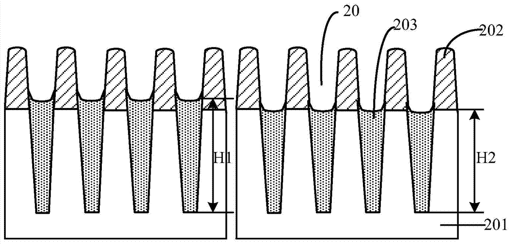
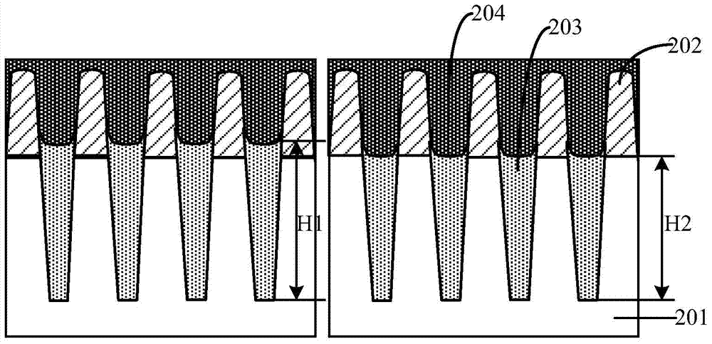
[0041] Attached below Figure 2a-2c The method for preparing the semiconductor device of the present invention is further described.

[0042] Firstly, step 201 is performed to provide a wafer in which a semiconductor substrate 201 is formed.

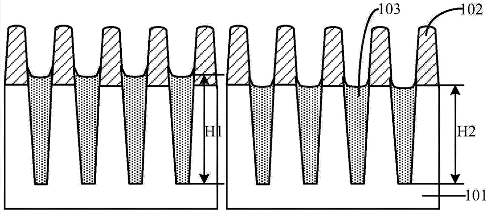
[0043] Specifically, such as Figure 2a As shown, wherein the wafer includes a central region and an edge region.

[0044] Wherein, the semiconductor substrate 201 may be at least one of the materials mentioned below: silicon, silicon-on-insulator (SOI), silicon-on-insulator (SSOI), silicon-germanium-on-insulator (S-SiGeOI) , silicon germanium on insulator (SiGeOI) and germanium on insulator (GeOI), etc.

[0045] Step 202 is performed to form a floating gate layer and a mask layer on the semiconductor substrate, and pattern them to form a floating gate structure 202 and a shallow trench.

[0046] Specifically, such as Figure 2a As shown, a floating gate layer is formed on the semiconductor substrate, and the floating gate layer may b...

Embodiment 2

[0077] The present invention also provides a semiconductor device, which is prepared by the method described in Embodiment 1. The isolation oxide in the edge region and central region of the semiconductor device prepared by the method of the present invention has a uniform thickness, so that the semiconductor device has a uniform threshold voltage and improves the performance and yield of the semiconductor device.

Embodiment 3

[0079] The present invention also provides an electronic device, including the semiconductor device described in Embodiment 2. Wherein, the semiconductor device is the semiconductor device described in Embodiment 2, or the semiconductor device obtained according to the preparation method described in Embodiment 1.

[0080] The electronic device of this embodiment can be any electronic product or equipment such as mobile phone, tablet computer, notebook computer, netbook, game console, TV set, VCD, DVD, navigator, camera, video recorder, voice recorder, MP3, MP4, PSP, etc. , can also be any intermediate product including the semiconductor device. The electronic device according to the embodiment of the present invention has better performance due to the use of the above-mentioned semiconductor device.


PUM


Abstract

The invention relates to a semiconductor device, a preparation method thereof, and an electronic device. The preparation method comprises: providing a semiconductor substrate including a central region and an edge region, wherein a plurality of floating gate structures are formed in the semiconductor substrate and shallow trench isolation structures are formed between the adjacent floating gate structures and downwardly extend to the semiconductor substrate; removing a part of oxide in the shallow trench isolation structures by using etching back in order to form a groove and expose a part of the sidewalls of the floating gate structures; depositing a covering layer in order to fill the groove and cover the floating gate structures; and removing a part of the covering layer by using wet etching in order to expose a part of the sidewalls of the floating gate structures again. The method further deposits the covering layer after a COPEN processing step, then removes the covering layer by using wet etching, and leaves a part of the covering layer at the edge region in order to compensate the thickness of the oxide in the edge area, thereby improving device performance and yield.

Description

technical field [0001] The invention relates to the field of semiconductor manufacturing, and in particular, the invention relates to a semiconductor device, a preparation method thereof, and an electronic device. Background technique [0002] With the increasing demand for high-capacity semiconductor storage devices, the integration density of these semiconductor storage devices has received more attention. In order to increase the integration density of semiconductor storage devices, many different methods have been adopted in the prior art, such as through Reducing the size of the memory cell and / or changing the structure of the unit to form more memory cells on a single wafer, as for the method of increasing the integration density by changing the cell structure, attempts have been made by changing the planar layout of the active region or changing Cell layout to reduce cell area. [0003] NAND flash memory is a better storage solution than hard disk drives. Since NAND ...

Claims


Application Information

Patent Timeline
Patent Type & Authority Patents(China)
IPC IPC(8): H01L27/11524
Inventor 陈亮仇圣棻
Owner SEMICON MFG INT (SHANGHAI) CORP
Why Eureka
Try Eureka