

Transistors and methods of forming them
A technology of transistors and dummy gate layers, applied in the field of transistors and their formation, can solve problems such as poor performance and poor morphology of high-K gate metal gate transistors, and achieve the effect of balanced threshold voltage and stable performance
- Summary
- Abstract
- Description
- Claims
- Application Information
AI Technical Summary
Problems solved by technology
Method used
Image

Examples
Embodiment Construction
[0035] As mentioned in the background art, the high-K metal gate transistor formed by the gate-last process has poor appearance and poor performance.
[0036] For details, please refer to Figure 1 to Figure 3 , Figure 1 to Figure 3 It is a schematic cross-sectional structure diagram of a process of forming a high-K metal gate transistor by a gate-later process according to an embodiment of the present invention.
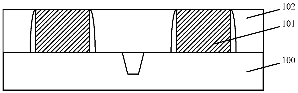
[0037] Please refer to figure 1 , providing a substrate 100, the surface of the substrate 100 has a dummy gate layer 101; a dielectric layer 102 is formed on the surface of the substrate 100, the dielectric layer 102 covers the sidewall of the dummy gate layer 101, and the dielectric Layer 102 exposes the top surface of the dummy gate layer 101 .
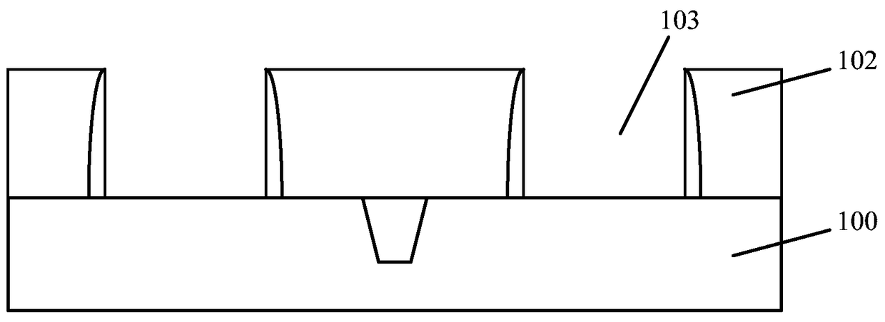
[0038] Please refer to figure 2 , removing the dummy gate layer 101 (such as figure 1 As shown), an opening 103 is formed in the dielectric layer 102 .
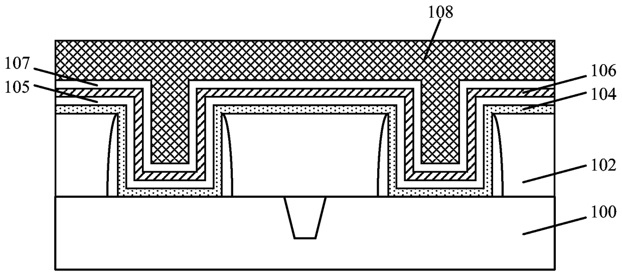
[0039] Please refer to image 3 , forming a gate dielectri...
PUM
 Abstract
Description
Claims
Application Information