Method for preparing two-dimensional metallic photonic crystal structure in large area through femtosecond laser direct writing
A metal photonic crystal and femtosecond laser technology, applied in laser welding equipment, metal processing equipment, welding equipment, etc., can solve the problems of complex preparation process, long process time, structural style and processing area limitation, etc. Simple, low cost, high efficiency effect
- Summary
- Abstract
- Description
- Claims
- Application Information
AI Technical Summary
Benefits of technology
Problems solved by technology
Method used
Image
Examples
Embodiment 1
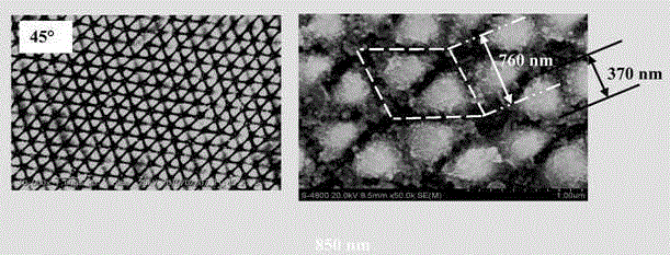
[0042] Such as figure 1 As shown, the horizontally linearly polarized laser 2 output from the femtosecond laser amplifier 1 with a repetition frequency of 1000 Hz, a pulse width of 50 femtoseconds, and a center wavelength of 800 nanometers is vertically incident on a YVO with a thickness of 1.26 mm after passing through a neutral attenuator 4 On the optical birefringent crystal 3, each incident pulse will be converted into two femtosecond laser pulses with the same central wavelength but the polarization directions are perpendicular to each other after exiting the crystal, wherein the polarization directions of the two beams are determined by the azimuth angle of the crystal It is determined that they are colinearly transmitted in space and the beam is focused by the same plano-convex cylindrical lens 4. By controlling the three-dimensional precision mobile platform 6, the surface of the sample material 5 to be processed is moved to a distance of 0-300 microns in front of the ...
Embodiment 2
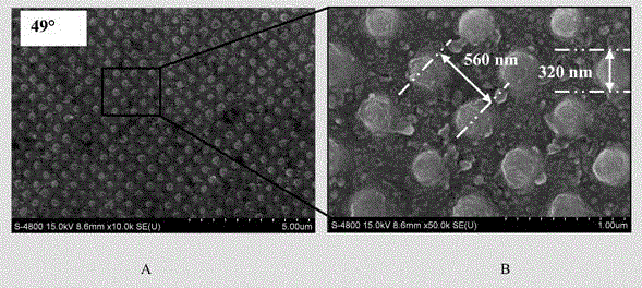
[0044] On the basis of the light path in embodiment 1, adopt neutral attenuation sheet to be incident to YVO 4 The femtosecond laser power on the crystal is attenuated and the YVO 4 The azimuth rotation of the crystal is adjusted to 49° to obtain a double-pulse femtosecond laser beam with output linear polarization directions perpendicular to each other and a central wavelength of 800 nanometers. Before they are incident on the plano-convex cylindrical lens, the measured total laser power is 180 mW, and the sample target surface is adjusted to the focal point of the lens. figure 2 Shown are scanning electron micrographs of microstructures obtained on the sample surface when the sample scanning speed is 0.02 mm / s, and the magnifications are 10,000 and 50,000 times, respectively. It can be seen from the figure that at this time, the surface of the sample forms a dot-like structure distributed in a two-dimensional periodic array, and the corresponding spatial period and cell di...
Embodiment 3
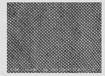
[0046] In the operation of Example 2, the width of the scribe line was increased to 0.15 mm to obtain a dot-shaped microstructure distributed in a two-dimensional periodic array within a large area. image 3 It is a scanning electron micrograph at 5000 times magnification.
PUM
 Abstract
Description
Claims
Application Information


