Array substrate, display panel and display device

A technology for array substrates and display panels, applied to static indicators, digital memory information, instruments, etc., can solve the problems of increasing the width of non-display areas, occupying space, and affecting the realization of narrow borders

Active Publication Date: 2015-12-09
BOE TECH GRP CO LTD +1
View PDF6 Cites 39 Cited by
  • Summary
  • Abstract
  • Description
  • Claims
  • Application Information

AI Technical Summary

Problems solved by technology

When the gate drive circuit is made on the array substrate, multiple signal lines and shift register units need to occupy a certain amount of space, resulting in an increase in the width of the non-display area, which affects the realization of narrow borders

Method used


Image

  • Array substrate, display panel and display device
  • Array substrate, display panel and display device
  • Array substrate, display panel and display device

Examples


Embodiment Construction

[0024] Specific embodiments of the present invention will be described in detail below in conjunction with the accompanying drawings. It should be understood that the specific embodiments described here are only used to illustrate and explain the present invention, and are not intended to limit the present invention.

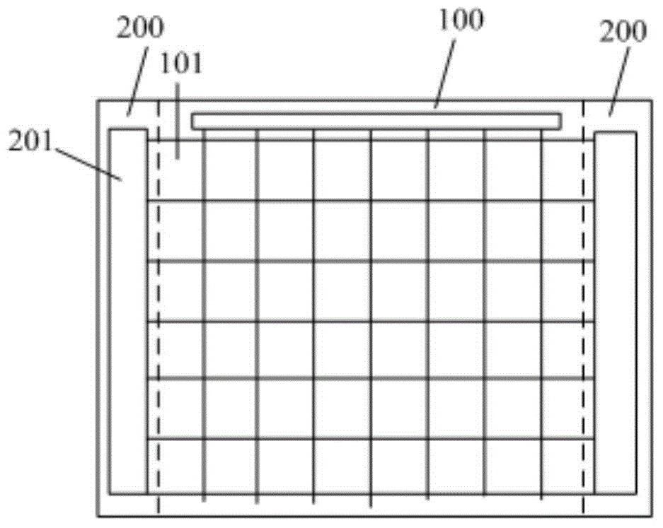
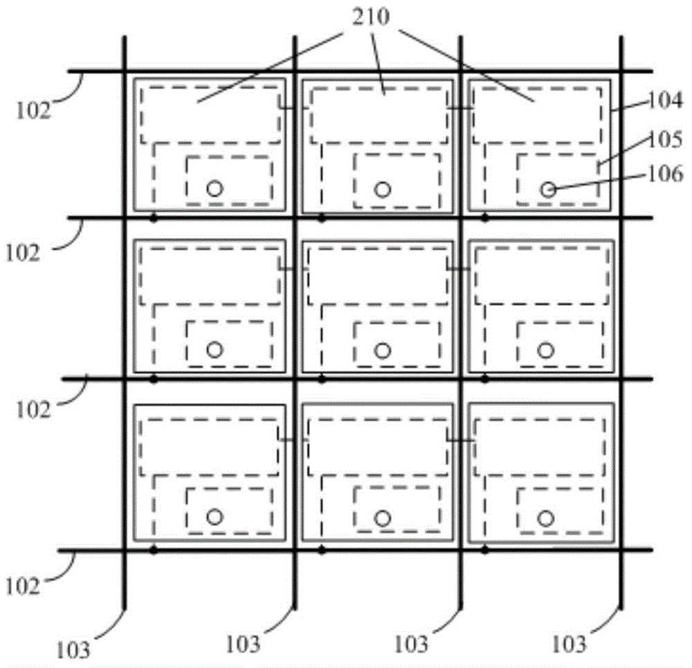
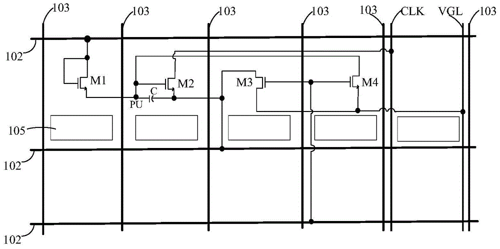
[0025] As an aspect of the present invention, an array substrate is provided, such as figure 2 and image 3 As shown, the array substrate includes a plurality of gate lines 102 and a plurality of data lines 103, the plurality of gate lines 102 and the plurality of data lines 103 define a plurality of pixel units, and the plurality of pixel units are arranged in multiple rows and columns, so The array substrate also includes a plurality of cascaded shift register units 210, the plurality of shift register units correspond to multiple rows of pixel units one by one, the shift register unit 210 includes a plurality of shift register elements, for any shift regist...


PUM


Abstract

The invention provides an array substrate, a display panel and a display device. The array substrate comprises multiple grating lines and multiple data lines, wherein the multiple grating lines and the multiple data lines define multiple pixel units. The array substrate also comprises multiple cascaded shift registration units, wherein the multiple shift registration units are in one-to-one correspondence with the multiple rows of pixel units; each shift registration unit comprises multiple shift registration elements; and as for any one shift registration unit, the at least one shift registration element in the shift registration unit is arranged in the at least one pixel unit in one row of pixel units of the corresponding shift registration unit. Compared with the prior art, the width of a non-display area occupied by the shift registration units is reduced, and realization of a narrow border is facilitated.

Description

technical field [0001] The present invention relates to the field of display technology, in particular to an array substrate, a display panel including the array substrate, and a display device including the display panel. Background technique [0002] Currently, the array substrate may include a display area 100 and a non-display area 200 , wherein the display area is defined by a plurality of gate lines and a plurality of data lines to define a plurality of pixel units 101 . Array substrate line drive (Gate Driver On Array, GOA) technology is to make the gate drive circuit in the non-display area on the array substrate. The gate driving circuit includes a plurality of cascaded shift register units and signal lines for providing signals (such as clock signals and frame start signals). When the gate drive circuit is fabricated on the array substrate, multiple signal lines and shift register units need to occupy a certain amount of space, resulting in an increase in the widt...

Claims


Application Information

Patent Timeline
IPC IPC(8): G09G3/32
CPCG11C19/28G09G3/3266G09G2310/0286G11C19/184H10K59/123G09G3/3258G09G3/3291G09G2300/0809G09G2310/0202G09G2310/062
Inventor 陈鹏张新霞
Owner BOE TECH GRP CO LTD
Why Eureka
Try Eureka