A camera module standard device and assembly method thereof

A camera module and standard device technology, applied in electrical components, image communication, color TV components, etc., can solve the problems of inability to standardize production, high material costs, etc., and achieve material saving, high yield and low cost. Effect

Inactive Publication Date: 2018-10-30
GUANGZHOU DALING INDAL
View PDF5 Cites 0 Cited by
  • Summary
  • Abstract
  • Description
  • Claims
  • Application Information

AI Technical Summary

Problems solved by technology

Due to different FPCs and connectors, the existing mobile phone rear cameras have a wide variety and cannot be produced in a standardized manner, which brings a lot of inventory risks and high material costs to mobile phone factories and module manufacturers.

Method used


Image

  • A camera module standard device and assembly method thereof
  • A camera module standard device and assembly method thereof
  • A camera module standard device and assembly method thereof

Examples


Embodiment Construction

[0022] Below in conjunction with accompanying drawing, invention is described in further detail.

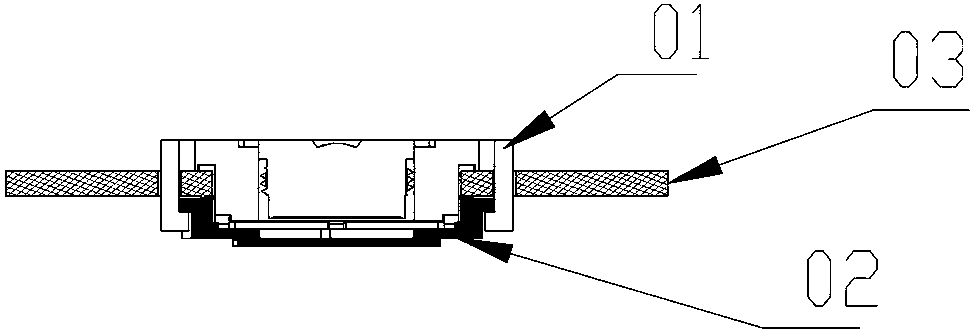
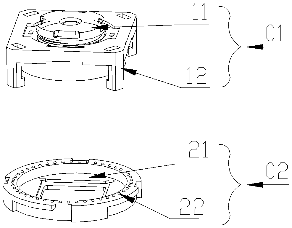
[0023] Such as figure 2 As shown, a camera module standard device includes a lens assembly 01 and a chip assembly 02; the lens assembly 01 includes a lens 11 and a lens holder 12; the chip assembly 02 includes a photosensitive chip 21 and a circular pad 22 . The lens 11 is connected to the lens holder 12 through threads. The photosensitive chip 21 and the circular pad 22 are connected by wafer bonding. The circular pad 22 has an annular metal pin and four annular relief holes, and the lens holder 12 has four male buckles. The lens assembly 01 and the chip assembly 02 are connected through the four male buckles of the lens holder 12 and the four annular relief holes of the circular pad 22 . The circular pad 22 is welded and attached to the main board of the digital product through the circular metal pin.

[0024] A camera module standard device assembly method, the specific ...


PUM


Abstract

The invention discloses a standard device of a camera module applicable to portable digital equipment, such as a mobile phone, a palm computer and a notebook computer, and an assembly method thereof, wherein the standard device comprises a chip component and a lens component; the chip component comprises a light sensitive chip and a circular bonding pad; and the lens component comprises a lens and a lens bracket. The standard device disclosed by the invention has the effects of being standardized, simple in structure, easy to assemble, energy-saving and environment friendly.

Description

technical field [0001] The invention relates to an image acquisition device, more specifically, relates to a standard camera module device and an assembly method thereof suitable for portable digital devices such as mobile phones, palmtop computers, and notebooks. Background technique [0002] A traditional camera module consists of a lens assembly (lens), a base (holder), an image sensor (CCD or CMOS) and a circuit board. The lens assembly corresponds to the photosensitive area of ​​the image sensor through the base and is assembled on the circuit board together. superior( figure 1 ); the image sensor is electrically connected to the internal circuit on the circuit board, and the image sensor and the circuit board convert the collected optical signal into a digital image signal, and then connect to the peripheral device (such as the main body of the mobile phone) through the connector on the circuit board. [0003] At present, when the camera leaves the factory, different ...

Claims


Application Information

Patent Timeline
Patent Type & Authority Patents(China)
IPC IPC(8): H04N5/225
Inventor 凌代年张春苑
Owner GUANGZHOU DALING INDAL
Why Eureka
Try Eureka