Silicon-based hybrid integration laser radar chip system

A hybrid integration, chip system technology, applied in the field of photoelectric detection, can solve the problems of complexity, large device size and bending radius, wide distribution of waveguide modes, etc., to achieve high thermal stability of gain, reduced chip cost, and reduced transceiver loss. Effect

Active Publication Date: 2019-07-09
SHANGHAI JIAOTONG UNIV
View PDF23 Cites 44 Cited by
  • Summary
  • Abstract
  • Description
  • Claims
  • Application Information

AI Technical Summary

Problems solved by technology

Finally, domestic patents titled optical phased array or laser phased array also began to increase in 2018, among which "a single-wavelength multi-line scanning system based on thermo-optic switch and silicon photonic phased array" (CN201810240144) attempted to Using a thermo-optical switch to route the output light to sub-arrays with different grating periods to achieve single-wavelength multi-line scanning, although this scheme avoids the use of wavelength tunable lasers, with the increase of the number of lines, the size of the switch, the sub-array The number and complexity of the control circuit will become a serious problem, limiting the beam precision of the optical phased array, the overall output power and on-chip insertion loss. In addition, the solution does not give the relevant design of the receiver; "based on wavelength division multiplexing "Integrated multi-beam optical phased array delay network" (CN201810424574), "A silicon-based multi-beam optical phased array antenna" (CN201810695911), respectively gave the realization of multi-beam optical phased array from two technical paths However, these works mainly focus on how to add a photonic circuit before the phased array to achieve a more complex beam control function, and do not give details on the design of the optical phased array itself and the composition of the laser radar system; " An optical phased array chip transmitter based on a metal slot waveguide" (CN201810619456) and "Wide-range scanning broadband laser phased array system" (CN201810558205) adopt different photonic antenna and decoupling design schemes. The spacing is reduced to between half and one wavelength, thereby increasing the antenna integration density on the transmitting side, and realizing a large-scale non-aliasing beam rotation, but the beam fineness of the phased array is inversely proportional to the total size of the phased array. Competing with the fine far-field resolution of traditional space optics, the total number of these high-density integrated photonic antennas will reach between thousands and tens of thousands, which greatly increases the complexity of the control circuit and the burden on the host computer
The earlier "Active Optical Phased Array Photonic Integrated Chip and Its Preparation Method" (CN 201611027155) mainly introduced the preparation process of photonic phased array based on the III / V family platform, because the III / V platform waveguide core-clad The refractive index difference between the layers is much smaller than that of the silicon base, the waveguide mode distribution is wider, the device size and bending radius are larger, and the coupling between channels is more serious. In addition, the cost of III / V chips is high, and the theoretical performance is not high in terms of chip design. In terms of scale output, there is no outstanding advantage
[0007] To sum up, although optical phased array lidar contends among hundreds of schools of thought, there are still many basic problems that have not been resolved: from the perspective of the platform, the pure silicon solution is limited by the two-photon absorption phenomenon (TPA, Two-Photon Absorption) existing in the silicon waveguide. ), it is difficult to support the high transmit power required for long-distance lidar applications; the work in the field of silicon nitride lacks low-power dynamic components, and only some passive components or static arrays for technology verification have been reported; pure III / V-group platforms are not suitable for the design and production of optical phased arrays in terms of performance and cost; the design of silicon insulator-III / V group material bonding has reliability and heat dissipation problems; in addition, some work reported on multi-layer platforms These works may have various reference values ​​in the sense of scientific research, but are not necessarily applicable to system applications in this field
Therefore, the chip system based on the multi-layer silicon-silicon nitride platform design in the present invention does not exist in the existing work content, and there are few works that have achieved the degree of completion of the laser radar system in the present invention and the flexibility of cursor sending and receiving.

Method used


Image

  • Silicon-based hybrid integration laser radar chip system
  • Silicon-based hybrid integration laser radar chip system
  • Silicon-based hybrid integration laser radar chip system

Examples


Embodiment Construction

[0048] In order to further clarify the purpose, technical solution and core advantages of this solution, the present invention will be further described in detail below in conjunction with the accompanying drawings and embodiments. Please note that the following specific examples are for illustrative purposes only, and are not intended to limit the present invention. At the same time, as long as the technical features involved in different implementation solutions in the embodiments do not constitute a conflict with each other, they can be combined with each other.

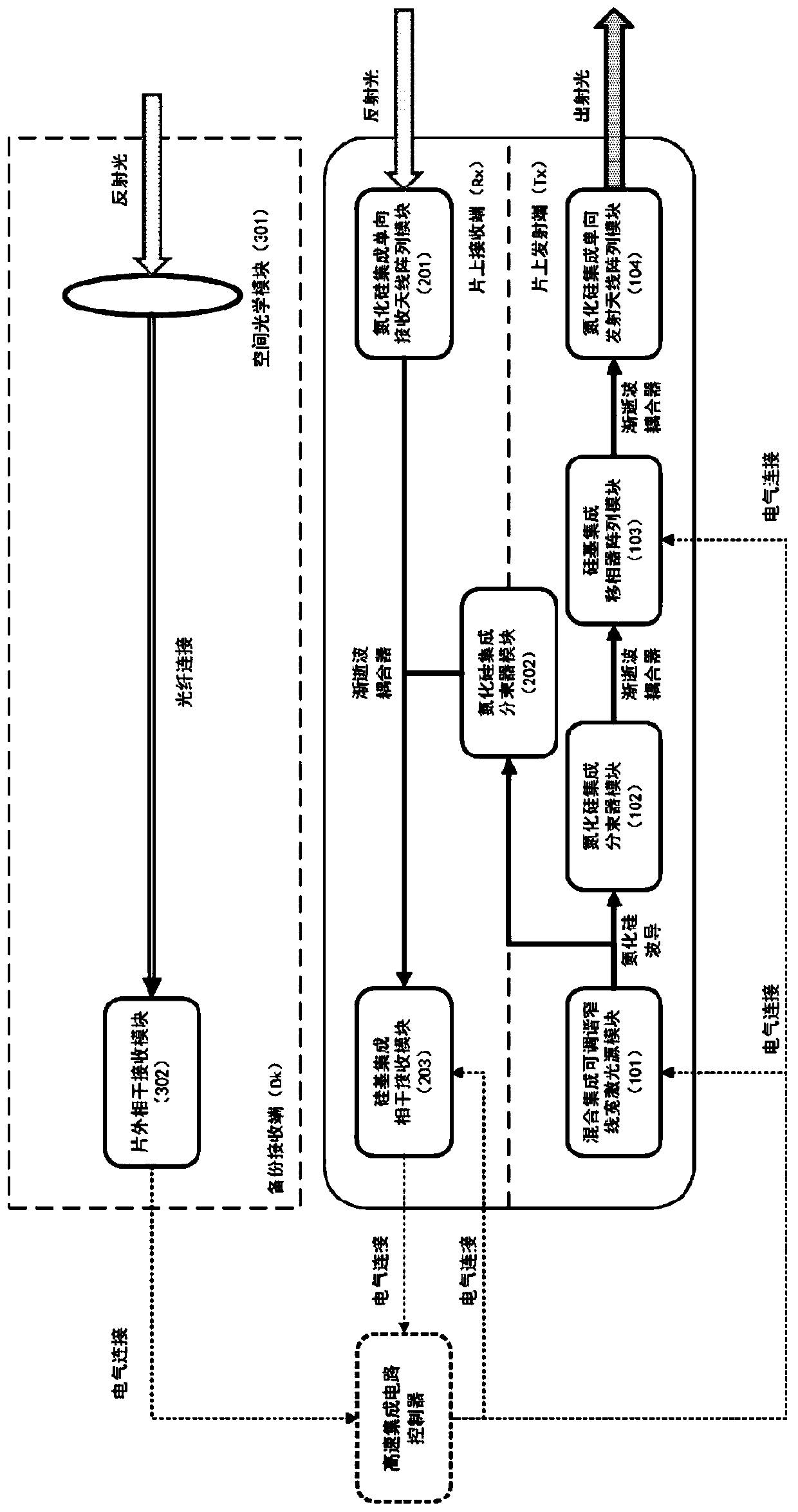
[0049] refer to figure 1 As shown, a silicon-based hybrid integrated laser radar chip system includes three main components: a transmitting end Tx, a receiving end Rx and a backup receiving end Bk; the transmitting end includes a hybrid integrated tunable narrow-linewidth laser source module 101, a nitride Silicon integrated beam splitter module 102, silicon-based integrated phase shifter array module 103 and sil...


PUM


Abstract

The invention discloses a silicon-based hybrid integration laser radar chip system. According to a light path sequence, the transmitting terminal of the system comprises a tunable narrow linewidth laser source, a silicon nitride beam splitter, a silicon-based phase shifter array and a silicon nitride one-way transmitting antenna array in sequence. According to a principle that the light path is reversible, the receiving terminal of the system comprises a silicon nitride one-way receiving antenna array, a silicon nitride beam splitter and a silicon-based coherence receiving module in sequence and also comprises a backup system and an electric domain control processing module. Each module on a silicon platform and a silicon nitride platform realizes multilayer single-chip integration with the help of a silicon / silicon nitride evanescent wave coupler, and a gain chip in a tunable laser source module and silicon nitride waveguide are subjected to hybrid integration through horizontal coupling. By use of the system, through multi-platform multi-field hybrid integration, the high-speed flexible wave beam formation, rotation and directivity receiving of a free space laser signal can be realized in a phased array way. The system does not contain movable devices, and has high integration density, good CMOS (Complementary Metal-Oxide-Semiconductor Transistor) compatibility, low large-scale volume production cost and extremely high practical value.

Description

technical field [0001] The invention belongs to the field of photoelectric detection, in particular to a silicon-based hybrid integrated laser radar chip system. Background technique [0002] LiDAR (Light Detection And Ranging), also known as LiDAR, is a remote sensing technology that uses a rotating laser beam to sample the environment at high speed to obtain three-dimensional depth information. Similar to traditional microwave radar, lidar also relies on the principle of transmitting and receiving electromagnetic waves reflected by targets. However, the working wavelength of lidar is much smaller than the former, which makes it inherently have higher resolution accuracy and larger instantaneous bandwidth. and greater integration potential. At the same time, with the vigorous development of military and civilian space telemetry and unmanned vehicles, the demand for high-speed acquisition of fine detection data from the environment is increasingly strong, which promotes the...

Claims


Application Information

Patent Timeline
Patent Type & Authority Applications(China)
IPC IPC(8): G01S7/481
CPCG01S7/481G01S17/42G02F1/292G01S7/4814G01S7/4817G01S7/4813G01S7/4818G01S17/88
Inventor 陆梁军许维翰周林杰刘娇陈建平
Owner SHANGHAI JIAOTONG UNIV
Why Eureka
Try Eureka