

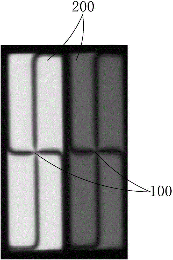
Pixel electrode structure
A pixel electrode and electrode technology, which is applied in the field of pixel electrode structure, can solve the problems affecting the transmittance and display effect of liquid crystal display panels, so as to improve the transmittance and display quality, increase the light transmission area, and reduce the "ten" The effect of glyph shadow
- Summary
- Abstract
- Description
- Claims
- Application Information
AI Technical Summary
Problems solved by technology
Method used
Image

Examples
Embodiment Construction
[0026] In order to further illustrate the technical means adopted by the present invention and its effects, the following describes in detail in conjunction with preferred embodiments of the present invention and accompanying drawings.
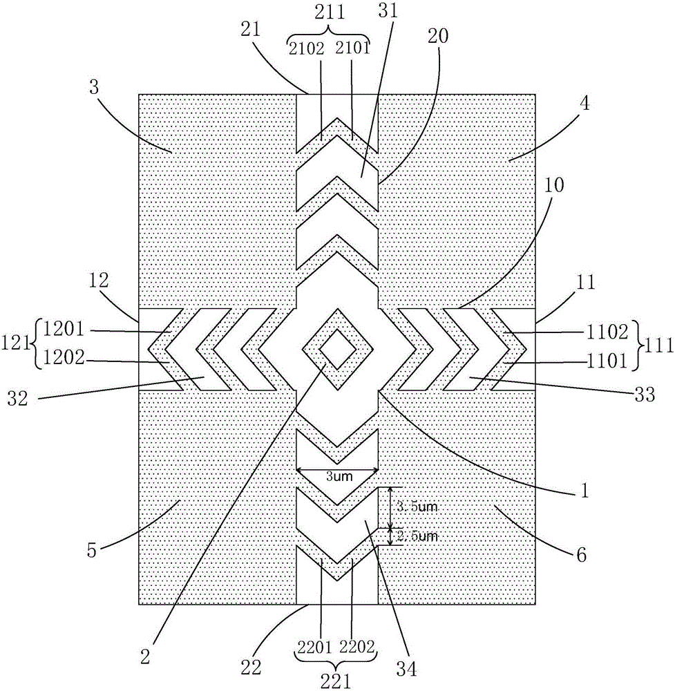
[0027] see figure 2 , the present invention provides a pixel electrode structure, including first, second, third, fourth electrodes 3, 4, 5, 6, a fifth electrode 21 connected between the first and second electrodes 3, 4, The sixth electrode 12 connected between the first and third electrodes 3, 5, the seventh electrode 11 connected between the second and fourth electrodes 4, 6, the seventh electrode 11 connected between the third and fourth electrodes 5, 6 The eighth electrode 22 between them, and the ninth electrode 2 located in the middle of the first to eighth electrodes 3 , 4 , 5 , 6 , 21 , 12 , 11 , 22 .
[0028] Specifically, the fifth to eighth electrodes respectively include a plurality of first, second, third, and fourth sub-electro...
PUM
| Property | Measurement | Unit |
|---|---|---|
| width | aaaaa | aaaaa |
| width | aaaaa | aaaaa |
Abstract
Description
Claims
Application Information