

Packaging substrate resistance welding processing method
A processing method and technology for packaging substrates, which are applied in the fields of circuits and electronics, and can solve the problems of restricting the performance of packaging substrates, the development of light, thin and miniaturization, the uneven surface of solder resist ink, and the flatness bottom.
- Summary
- Abstract
- Description
- Claims
- Application Information
AI Technical Summary
Problems solved by technology
Method used
Image

Examples
Embodiment Construction
[0023] The present invention will be described in further detail below, but the embodiments of the present invention are not limited thereto.
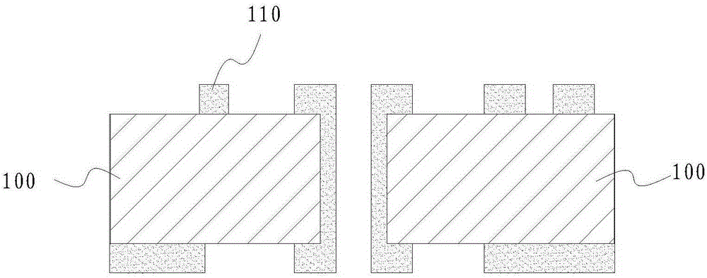
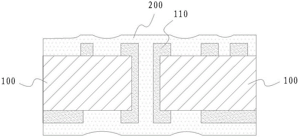
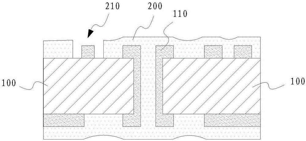
[0024] In the traditional packaging substrate solder mask printing process, since the surface of the package substrate is covered with graphics and the substances in the solder mask ink volatilize during the curing process of the solder mask ink, the solder mask surface of the package substrate is uneven, and the unevenness is generally several microns. The quality requirement that the flatness error is less than the micron level cannot be realized.
[0025] In the solder resist processing method of the packaging substrate in this embodiment, by adjusting the printing times of the solder resist ink and controlling the parameters of exposure, development and curing, the error of the flatness of the solder resist of the package substrate product is less than micron level. Include steps:
[0026] (A) First printing
[0027] Before the f...
PUM
 Abstract
Description
Claims
Application Information