Array substrate, display panel and method for manufacturing array substrate

A technology of array substrates and color film substrates, applied in static indicators, instruments, nonlinear optics, etc., can solve the problems of complex structure, high cost, and cumbersome preparation process of display devices, and achieve reduced production costs, simple structure, and simplified The effect of the production process

Active Publication Date: 2018-10-23
XIAMEN TIANMA MICRO ELECTRONICS +1
View PDF5 Cites 0 Cited by
  • Summary
  • Abstract
  • Description
  • Claims
  • Application Information

AI Technical Summary

Problems solved by technology

[0004] The present invention provides an array substrate, a display panel and a method for manufacturing the array substrate, so as to solve the problems of complex structure, cumbersome preparation process and high cost of display devices in the prior art

Method used


Image

  • Array substrate, display panel and method for manufacturing array substrate
  • Array substrate, display panel and method for manufacturing array substrate
  • Array substrate, display panel and method for manufacturing array substrate

Examples


Embodiment Construction

[0029] The present invention will be further described in detail below in conjunction with the accompanying drawings and embodiments. It should be understood that the specific embodiments described here are only used to explain the present invention, but not to limit the present invention. In addition, it should be noted that, for the convenience of description, only some structures related to the present invention are shown in the drawings but not all structures.

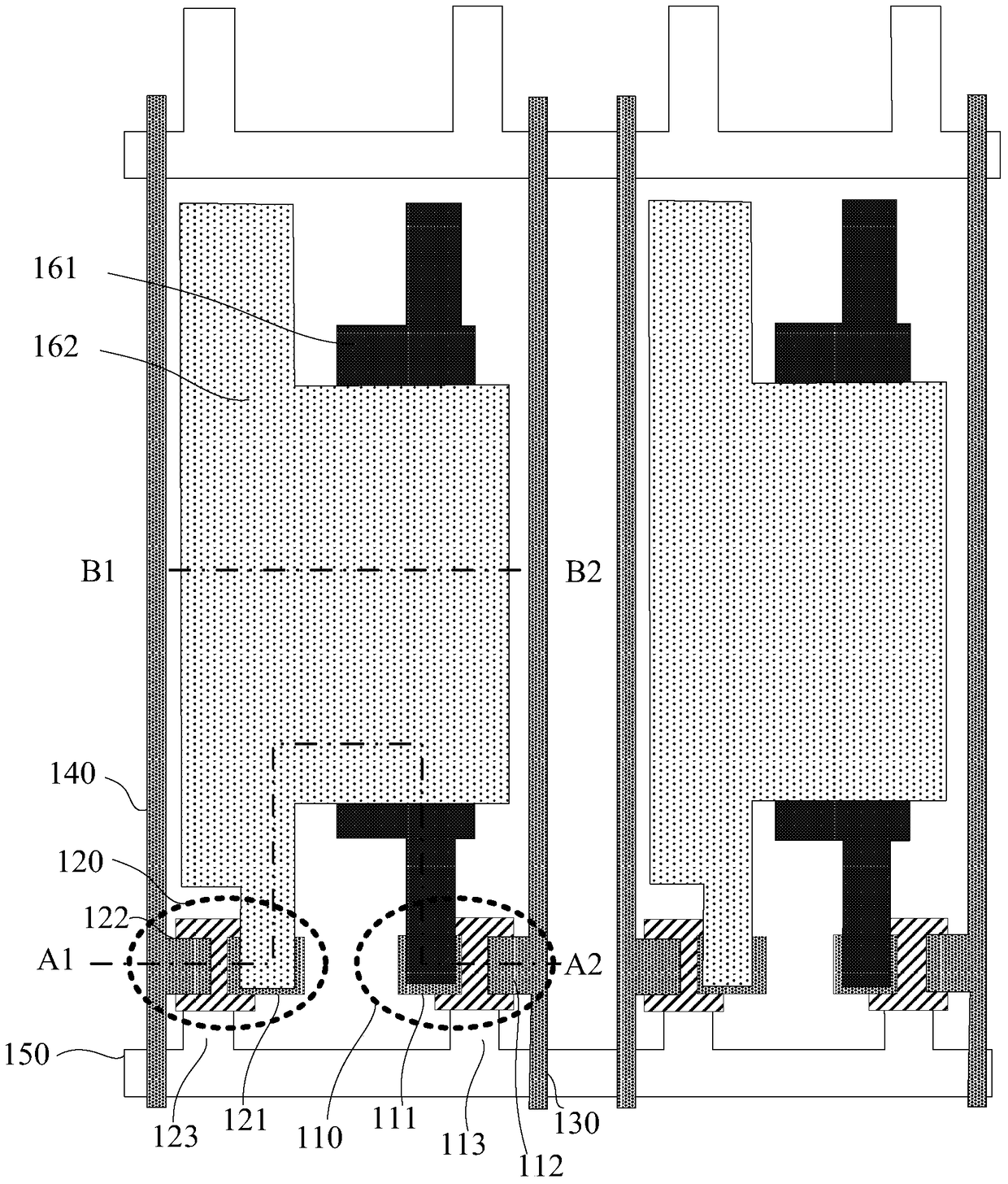
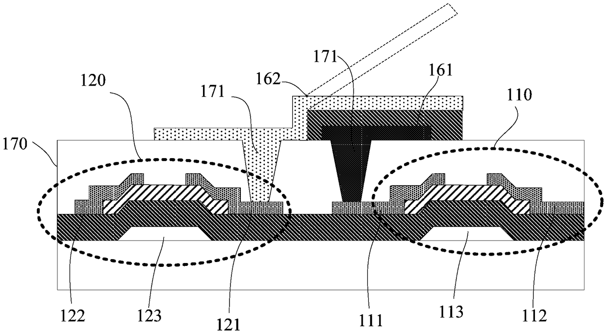
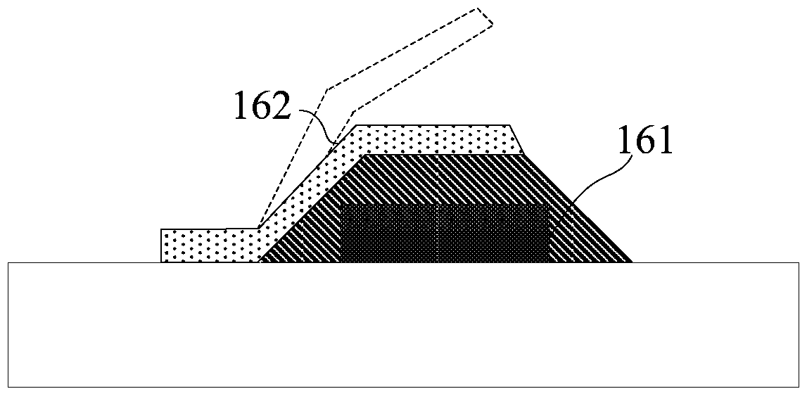
[0030] figure 1 It is a schematic top view structure diagram of an array substrate provided by an embodiment of the present invention, figure 2 Provided along the embodiment of the present invention figure 1 Schematic diagram of the cross-sectional structure in the direction of A1-A2, image 3 Provided along the embodiment of the present invention figure 1 Schematic diagram of the cross-sectional structure in the B1-B2 direction. Such as Figure 1-Figure 3 As shown, the array substrate provided by the embodi...


PUM


Abstract

The invention discloses an array substrate, a display panel and a manufacturing method of the array substrate. The array substrate comprises multiple pixel units. A first data line and a second data line are respectively arranged on the two sides of each pixel unit. Each pixel unit comprises a first thin film transistor, a second thin film transistor, a transparent reference layer and a non-transparent deformation layer located above the transparent reference layer and insulated from the transparent reference layer, wherein the output ends of the first thin film transistors are electrically connected with the transparent reference layers, the input ends of the first thin film transistors are electrically connected with the corresponding first data lines, and the control ends of the first thin film transistors are electrically connected with corresponding scanning lines. The output ends of the second thin film transistors are electrically connected with the non-transparent deformation layers, the input ends of the second thin film transistors are electrically connected with the corresponding second data lines, and the control ends of the second thin film transistors are electrically connected with corresponding scanning lines. The display panel manufactured by utilizing the array substrate is simple in structure and low in production cost.

Description

technical field [0001] Embodiments of the present invention relate to the field of display technology, and in particular, to an array substrate, a display panel, and a method for manufacturing the array substrate. Background technique [0002] The display device is widely used in people's work and life because of its advantages of being able to present information to people intuitively, making the transmission and communication of information between people more convenient and quick. [0003] With the continuous development of display technology, display devices have experienced the development of display images from black and white to color, from blurred to clear, from bulky and heavy to thin and light since their birth, and the performance of display devices has also been continuously improved. However, various display devices currently mainstream, such as LCD (Liquid Crystal Display) liquid crystal displays, still generally have problems such as complex structures, cumber...

Claims


Application Information

Patent Timeline
Patent Type & Authority Patents(China)
IPC IPC(8): G02F1/01G09G3/34
CPCG02F1/0128G09G3/3433
Inventor 杨育青王磊
Owner XIAMEN TIANMA MICRO ELECTRONICS
Why Eureka
Try Eureka