Array substrate and making method thereof, display panel and display device

A technology of an array substrate and a manufacturing method, applied in the display field, can solve problems such as uneven diffusion, achieve the effects of reducing drop, solving uneven diffusion of PI in an alignment layer, and improving display quality

Active Publication Date: 2016-02-03
BOE TECH GRP CO LTD +1
View PDF3 Cites 24 Cited by
  • Summary
  • Abstract
  • Description
  • Claims
  • Application Information

AI Technical Summary

Problems solved by technology

[0004] The invention provides an array substrate and its manufacturing method, a display panel, and a display device, which are used to reduce the gap between the upper surface of the via hole in the array substrate and the transparent conductive layer around the via hole, thereby solving the uneven diffusion of PI in the alignment layer problem, improve display quality

Method used


Image

  • Array substrate and making method thereof, display panel and display device
  • Array substrate and making method thereof, display panel and display device
  • Array substrate and making method thereof, display panel and display device

Examples


Embodiment 1

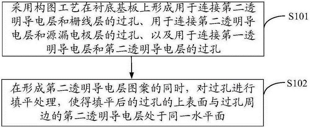
[0043] see figure 1 , a method for manufacturing an array substrate provided by an embodiment of the present invention, the method includes:

[0044] S101, using a patterning process to form a via hole for connecting the second transparent conductive layer and the gate line layer, a via hole for connecting the second transparent conductive layer and the source-drain electrode layer, and a via hole for connecting the first via holes in the transparent conductive layer and the second transparent conductive layer;

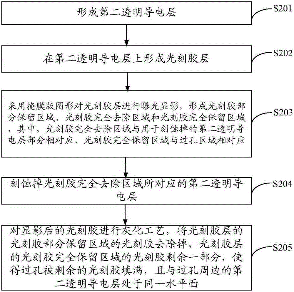
[0045] S102 , while forming the pattern of the second transparent conductive layer, perform filling and leveling processing on the via hole, so that the top surface of the filled via hole is at the same level as the second transparent conductive layer around the via hole.

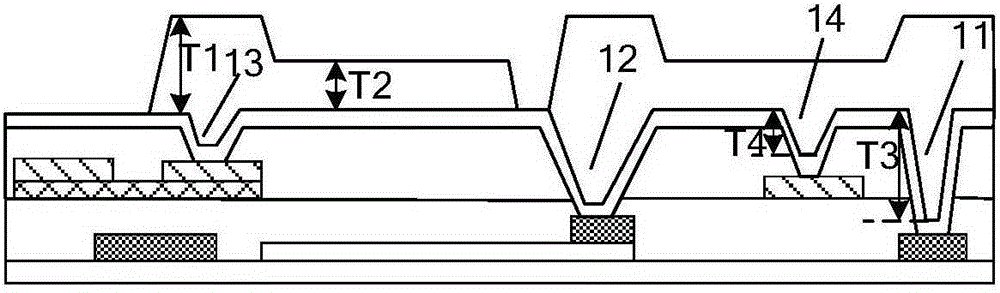
[0046]It should be noted that the first transparent conductive layer in the embodiment of the present invention refers to the common electrode layer, and the second transparent conductive layer re...


PUM


Abstract

The invention discloses an array substrate and a making method thereof, a display panel and a display device in order to reduce the height difference between the transparent conductive layer on the upper surface of a via hole and the transparent conductive layer around the via hole in an array substrate, solve the problem that diffusion of polyimide film PI in the alignment layer is uneven and improve the display quality. The making method of the array substrate is characterized by comprising the following steps: using a composition process to a form a via hole used for connecting a second transparent conductive layer and a gate line layer, a via hole used for connecting the second transparent conductive layer and a source and drain electrode layer and a via hole used for connecting a first transparent conductive layer and the second transparent conductive layer; and while the pattern of the second transparent conductive layer is formed, filling and leveling up the via holes to make the second transparent conductive layer on the upper surfaces of the via holes and the second transparent conductive layer around the via holes in the same horizontal plane.

Description

technical field [0001] The present invention relates to the field of display technology, in particular to an array substrate and a manufacturing method thereof, a display panel, and a display device. Background technique [0002] In the manufacturing process of thin film transistor liquid crystal display panel (TFT-LCD), holes need to be drilled inside and around the panel (Panel), for example, for connecting the transparent conductive layer (ITO) and the grid line layer, or connecting the transparent conductive layer and Source-drain metal, or a via hole connecting the transparent conductive layer and the common electrode line. Moreover, due to the uneven morphology in the via hole and the surrounding area of ​​the via hole, the alignment layer polyimide film (PolyimideFilm, PI) is coated, and the problem of uneven diffusion of PI in the alignment layer occurs, which seriously affects the local area of ​​the display area. Displays the picture quality of the screen. For ex...

Claims


Application Information

Patent Timeline
Patent Type & Authority Applications(China)
IPC IPC(8): H01L27/12H01L21/77G02F1/1362
CPCG02F1/133345H01L27/124G02F1/136227G02F1/136286G02F1/136236G02F1/13439G02F1/1368G02F2201/121G02F2201/123
Inventor 白金超郭会斌刘耀丁向前
Owner BOE TECH GRP CO LTD
Why Eureka
Try Eureka