A vertically integrated unit diode chip
A technology of integrated units and diodes, applied in electrical components, semiconductor devices, circuits, etc., can solve the problems of LED light efficiency, heat dissipation and stability limitations, and achieve increased effective light output area, large heat dissipation area, and high photoelectric conversion efficiency. Effect
- Summary
- Abstract
- Description
- Claims
- Application Information
AI Technical Summary
Problems solved by technology
Method used
Image

Examples
Embodiment 1
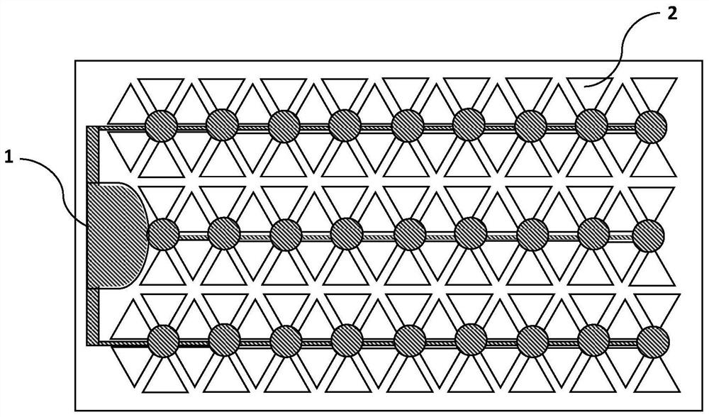
[0049] This embodiment provides a vertically integrated unit diode chip, such as image 3 with 7 As shown, it includes: n-type electrode 1, diode mesa structure 2, diode mesa structure 2 includes 6 rows of 102 triangular diode units of equal size and uniform distribution, and the length of the diode unit along the x-axis direction is 40 microns. The diode mesa structure adopts a triangular arrangement, and the size of the mesa structure is smaller than the diffusion length of the current injection. The electrode material adopts non-light-absorbing materials such as ITO, Al, Ag, etc. to improve light efficiency. The width of the electrode line is 0.001-20 microns, and the thickness is 0.001-10 microns.
[0050] When the vertically integrated unit diode chip emits light waves of UVC, UVB, UVA, purple light, blue light, green light, yellow light, and red light: the material of the unit diode chip is Alx1Iny1Gaz1N, 1≥x1, y1, z1≥0; the lining The bottom is a planar substrate, or ...
Embodiment 2
[0054] This embodiment provides another vertically mounted integrated unit diode chip, such as Figure 4 with 7 shown, including:
[0055] The n-type electrode 1, the diode mesa structure 2, the diode mesa structure 2 includes 6 rows of 6 uniformly distributed rectangular diode units, and the length of the diode units along the x-axis direction is 40 microns. The diode mesa structure is arranged in a rectangle, and the size of the mesa structure is smaller than the diffusion length of the current injection. The electrode material adopts non-light-absorbing materials such as ITO, Al, Ag, etc. to improve light efficiency. The width of the electrode line is 0.001-20 microns, and the thickness is 0.001-10 microns.
[0056] When the vertically integrated unit diode chip emits light waves of UVC, UVB, UVA, purple light, blue light, green light, yellow light, and red light: the material of the unit diode chip is Alx1Iny1Gaz1N, 1≥x1, y1, z1≥0; the lining The bottom is a planar subs...
Embodiment 3
[0060] This embodiment provides another vertically mounted integrated unit diode chip, such as Figure 5 with 7 shown, including:
[0061] The n-type electrode 1, the diode mesa structure 2, the diode mesa structure 2 includes 6 rows of 56 square diode units of equal size and uniform distribution. The diode mesa structure adopts a square arrangement, and the size of the mesa structure is smaller than the diffusion length of the current injection. The electrode material adopts non-light-absorbing materials such as ITO, Al, Ag, etc. to improve light efficiency. The width of the electrode line is 0.001-20 microns, and the thickness is 0.001-10 microns.
[0062] When the vertically integrated unit diode chip emits light waves of UVC, UVB, UVA, purple light, blue light, green light, yellow light, and red light: the material of the unit diode chip is Alx1Iny1Gaz1N, 1≥x1, y1, z1≥0; the lining The bottom is a planar substrate, or a patterned substrate; the substrate material is sap...
PUM
| Property | Measurement | Unit |
|---|---|---|
| width | aaaaa | aaaaa |
| thickness | aaaaa | aaaaa |
| diameter | aaaaa | aaaaa |
Abstract
Description
Claims
Application Information
 - R&D
- Intellectual Property
- Life Sciences
- Materials
- Tech Scout
- Unparalleled Data Quality
- Higher Quality Content
- 60% Fewer Hallucinations
Browse by: Latest US Patents, China's latest patents, Technical Efficacy Thesaurus, Application Domain, Technology Topic, Popular Technical Reports.
© 2025 PatSnap. All rights reserved.Legal|Privacy policy|Modern Slavery Act Transparency Statement|Sitemap|About US| Contact US: help@patsnap.com