Supercharge Your Innovation With Domain-Expert AI Agents!

PCB board information collection equipment

A PCB board and information collection technology, applied in electrical components, printed circuit manufacturing, printed circuit and other directions, can solve the problems of high labor participation, low productivity, time-consuming and laborious, and achieve the effect of improving production efficiency and adjusting quickly.

Active Publication Date: 2018-06-12
PKU HKUST SHENZHEN HONGKONG INSTITUTION +1
View PDF4 Cites 0 Cited by
  • Summary
  • Abstract
  • Description
  • Claims
  • Application Information

AI Technical Summary

Problems solved by technology

[0003] The purpose of the present invention is to provide a PCB board information collection device, aiming to solve the problems of too much manual participation, time-consuming and labor-intensive, and low productivity when the existing fixture with a suction cup clamps a PCB board

Method used


Image

  • PCB board information collection equipment
  • PCB board information collection equipment
  • PCB board information collection equipment

Examples


Embodiment Construction

[0023] In order to make the objectives, technical solutions, and advantages of the present invention clearer, the following further describes the present invention in detail with reference to the accompanying drawings and embodiments. It should be understood that the specific embodiments described herein are only used to explain the present invention, but not to limit the present invention.

[0024] Such as Figure 1~8 Shown are the preferred embodiments provided by the present invention.

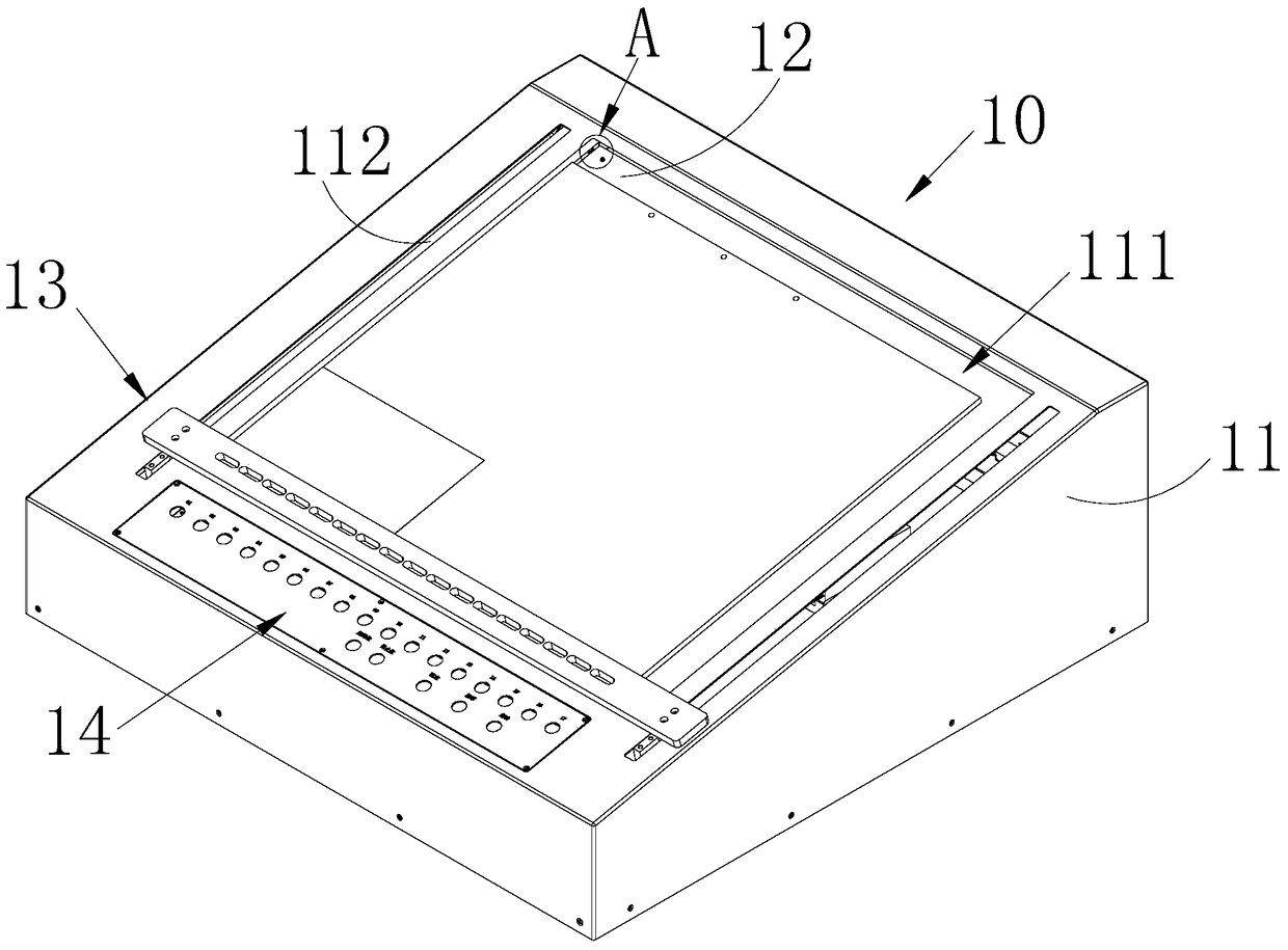
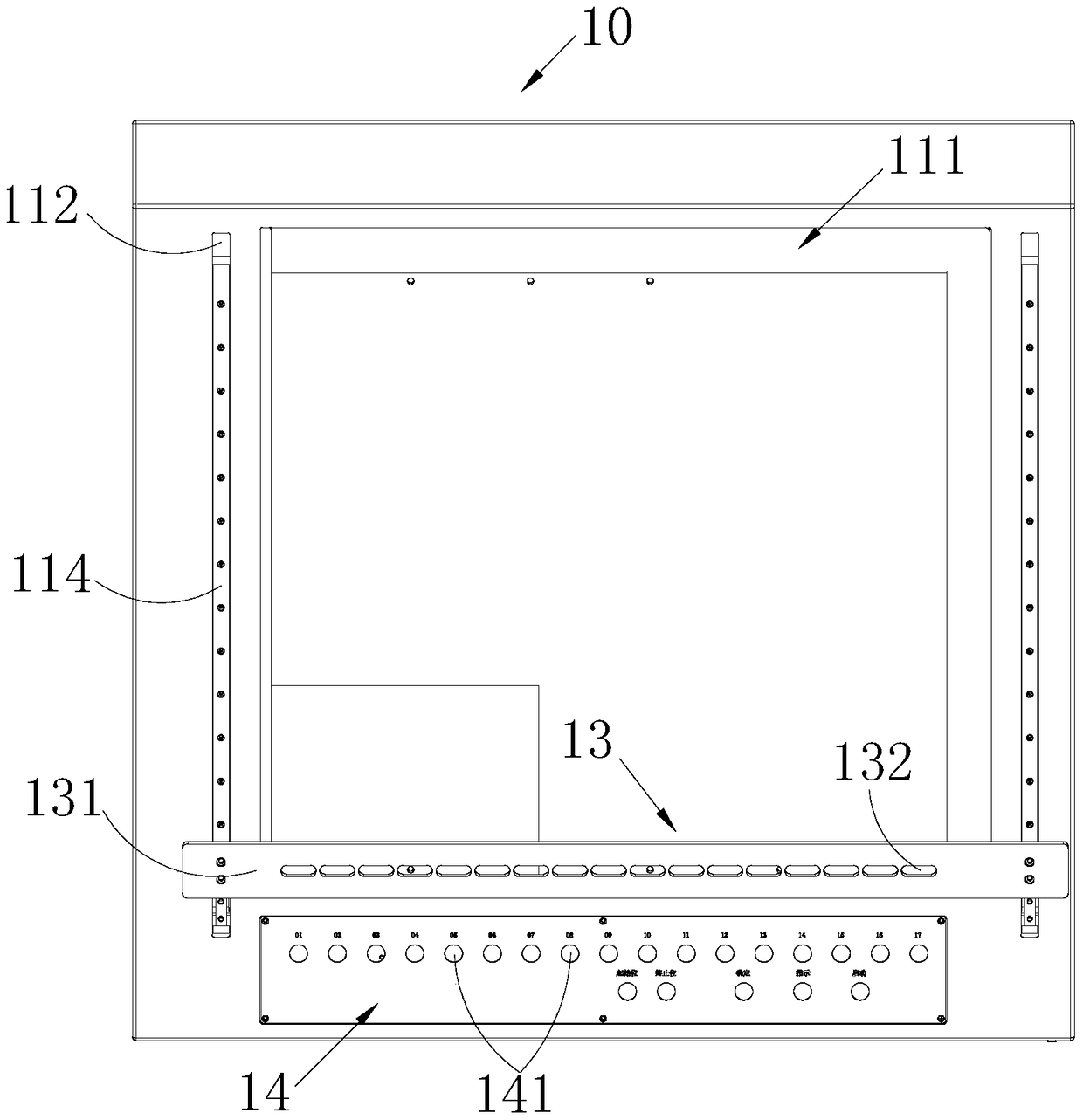
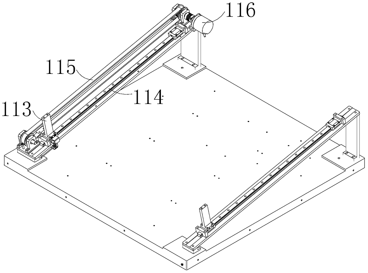
[0025] Such as figure 1 As shown, the PCB board information collection device 10 provided in this embodiment is used in conjunction with a fixture with suction cups in the PCB board production and processing process; the PCB board information collection device 10 is used to collect hole position information on the PCB board, The information is generated into a work file, and the control center uses the work file to control and adjust the opening or closing settings of multiple suction cups on th...


PUM


Abstract

The invention relates to the technical field of PCB industrial devices and provides a PCB information acquisition device. The PCB information acquisition device comprises a table body, wherein a light source is arranged in the table body; and a light transmission layer used for placing a PCB, an acquisition module used for receiving position information of light rays penetrating through the PCB and feeding back or converting the position information of the light rays into position information of holes in the PCB, and an input module used for inputting the position information of the holes in the PCB, acquired by the acquisition module and generating a working file by the position information of the holes are arranged on the upper surface of the table body. The light rays emitted by the light source of the PCB information acquisition device penetrate through the light transmission layer, irradiate the PCB and penetrate through the holes in the PCB, the acquisition module receives the light rays penetrating through the PCB and converts the light rays into the position information of the holes in the PCB, and the input module generates the working file by the position information of the holes, so that the number of suction cups for clamps and the distance between two rows of suction cups can be known, and the problems of too high artificial participation degree, time and labor waste and low productivity when existing suction cups clamp the PCB are solved.

Description

Technical field [0001] The invention belongs to the technical field of PCB industry equipment, and particularly relates to a PCB board information collection device. Background technique [0002] At present, in the production and processing process of PCB boards, the clamping of PCB boards is generally realized by using a fixture with multiple suction cups. When the clamping is a non-porous PCB board, the clamping can be easily completed by the fixture through the suction cup; When picking a porous PCB board, the position of the hole on the PCB board will affect the suction of the suction cup, making the suction force of the suction cup insufficient. Therefore, the suction position of the suction cup on the PCB board needs to be adjusted to a non-porous position, and When the holes on the PCB board are dense and irregular, it is necessary to carefully, carefully, align and adjust the suction position of each suction cup through manual visual inspection. Even when the weight of th...

Claims


Application Information

Patent Timeline
Patent Type & Authority Patents(China)
IPC IPC(8): H05K3/00
Inventor 蒋仕龙黄海李峰
Owner PKU HKUST SHENZHEN HONGKONG INSTITUTION
Features
  • R&D
  • Intellectual Property
  • Life Sciences
  • Materials
  • Tech Scout
  • Unparalleled Data Quality
  • Higher Quality Content
  • 60% Fewer Hallucinations
Learn More