Electronic device shell, manufacturing method of electronic device shell and electronic device

A technology of electronic devices and manufacturing methods, applied in the direction of casings/cabinets/drawer parts, etc., can solve the problems of affecting user experience, high cost, inconvenient buttoning, etc., to improve user experience and reduce use thickness , to ensure the effect of metal appearance

Inactive Publication Date: 2016-02-03
GUANGDONG OPPO MOBILE TELECOMM CORP LTD
View PDF4 Cites 13 Cited by
  • Summary
  • Abstract
  • Description
  • Claims
  • Application Information

AI Technical Summary

Problems solved by technology

[0003] Using stamping and CNC to process aluminum alloy, the aluminum alloy used is relatively thick (the thickness of aluminum alloy is generally 1.0-2.5mm), the cost will be relatively high, and it is inconvenient to make complex structures such as buckles, which affects user experience

Method used


Image

  • Electronic device shell, manufacturing method of electronic device shell and electronic device
  • Electronic device shell, manufacturing method of electronic device shell and electronic device
  • Electronic device shell, manufacturing method of electronic device shell and electronic device

Examples


Embodiment 1

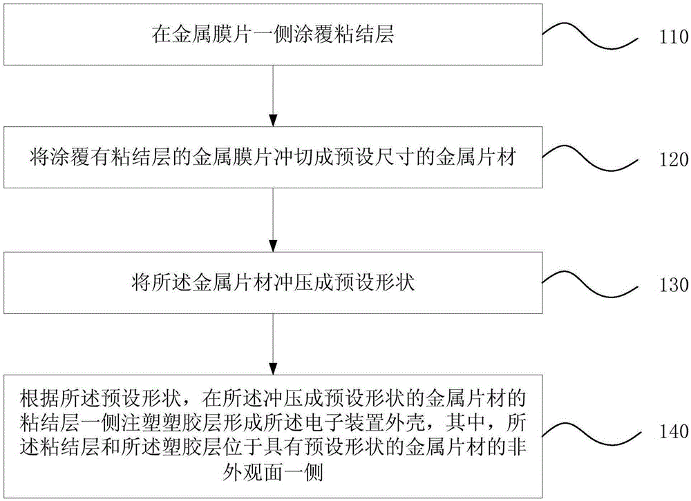
[0021] figure 1 It is a flow chart of a method for manufacturing an electronic device housing provided in Embodiment 1 of the present invention, and the method specifically includes the following steps:

[0022] Step 110, coating an adhesive layer on one side of the metal diaphragm.

[0023] Step 120 , punching the metal diaphragm coated with the adhesive layer into metal sheets of predetermined size.

[0024] The metal diaphragm coated with the adhesive layer is punched into metal sheets of predetermined size according to the size of the housing of the electronic device to be processed.

[0025] Step 130, stamping the metal sheet into a preset shape.

[0026] Specifically, the metal sheet punched into a preset size is put into a punching die, and punched into a preset shape, and the preset shape is the same as the shape of the housing of the electronic device to be processed. Optionally, multi-stage stamping can also be carried out due to the difference in appearance chara...

Embodiment 2

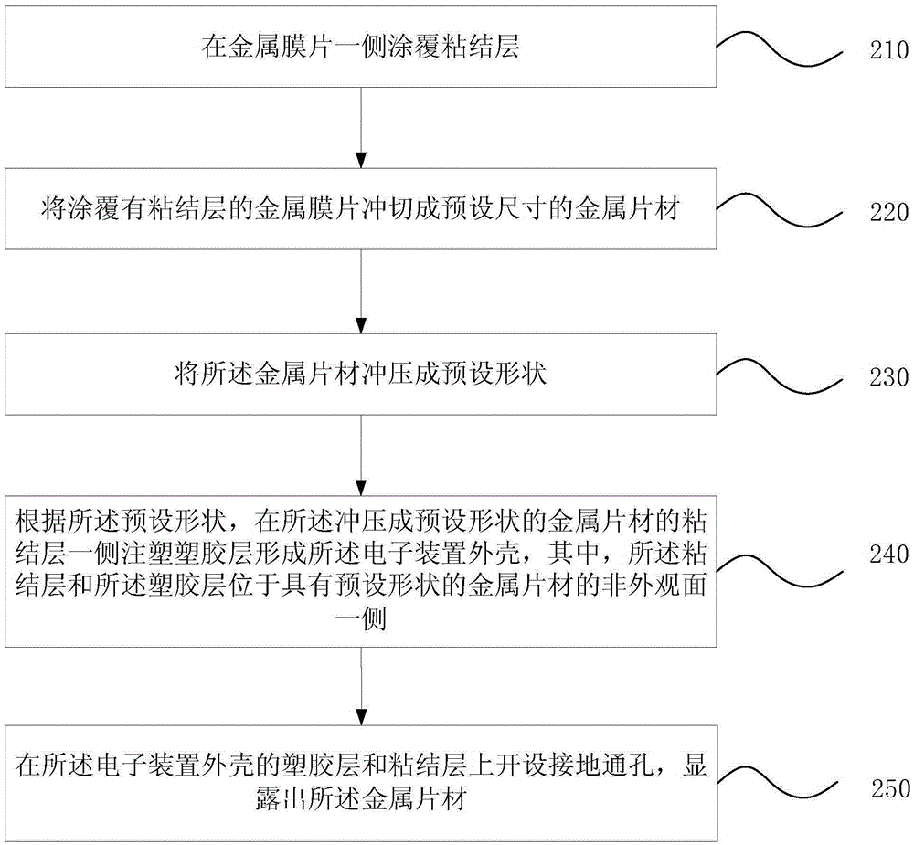
[0043] figure 2 It is a flow chart of a method for manufacturing an electronic device casing provided by Embodiment 2 of the present invention. This embodiment is based on the embodiment. After step 140, it preferably further includes: A ground via hole is opened on the junction layer to expose the metal sheet. see figure 2 , the method specifically includes the following steps:

[0044] Step 210, coating an adhesive layer on one side of the metal diaphragm;

[0045] Step 220, punching the metal diaphragm coated with the adhesive layer into a metal sheet of a predetermined size;

[0046] Step 230, stamping the metal sheet into a preset shape;

[0047] Step 240, according to the preset shape, inject a plastic layer on one side of the adhesive layer of the metal sheet punched into the preset shape to form the housing of the electronic device, wherein the adhesive layer and the plastic layer On the non-appearance side of a metal sheet with a predetermined shape.

[0048] ...

Embodiment 3

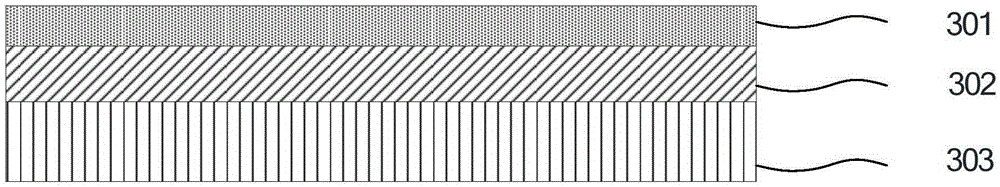
[0052] image 3 It is a schematic cross-sectional view of an electronic device housing in Embodiment 3 of the present invention. The electronic device housing of this embodiment can be made by any method provided in this embodiment. See image 3 , the electronic device housing includes: a metal sheet 301 with a preset shape, an adhesive layer 302 and a plastic layer 303; wherein, the non-appearance surface of the metal sheet 301 with a preset shape passes through the adhesive layer 302 is connected to the plastic layer 303 , and the shape of the plastic layer 303 matches the preset shape of the metal sheet 301 .

[0053] The technical solution of this embodiment provides an electronic device housing, which includes a metal sheet with a preset shape, an adhesive layer, and a plastic layer; wherein, the non-appearance of the metal sheet with a preset shape The surface is connected to the plastic layer through the adhesive layer, and the shape of the plastic layer matches the pr...


PUM


Abstract

The invention discloses an electronic device shell, a manufacturing method of the electronic device shell and an electronic device. The method comprises the following steps: applying an adhering layer to one side of a metal diaphragm; punching the metal diaphragm with the adhering layer into a metal sheet with a preset size; stamping the metal sheet into a preset shape; and according to the preset shape, injecting a plastic layer on the adhering layer side of the metal sheet stamped into the preset shape, so as to form the electronic device shell, wherein the adhering layer and the plastic player are placed on the non-appearance face side of the metal sheet which is of the preset shape. Since the structural thickness of the metal diaphragm is relatively low, the production cost of the electronic device shell can be reduced; in addition, the plastic layer formed in an injection molding way on the adhering layer side of the metal sheet can be used at complicated fastening positions so that the electronic device shell and the electronic device can be fastened together tightly and hardly separated, thus improving the user experience.

Description

technical field [0001] Embodiments of the present invention relate to electronic equipment technology, and in particular, to an electronic device casing, a manufacturing method, and an electronic device. Background technique [0002] Usually, the housing of the electronic device is processed by stamping and computer numerical control (CNC) to remove the aluminum alloy to make the shape features, and then the surface of the battery device housing is treated by sandblasting and anodizing. to achieve a specific appearance. [0003] Using stamping and CNC to process aluminum alloy, the aluminum alloy used is relatively thick (the thickness of aluminum alloy is generally 1.0-2.5mm), the cost will be relatively high, and it is inconvenient to make complex structures such as buckles, which affects the user experience. Contents of the invention [0004] The invention provides an electronic device casing, a manufacturing method and the electronic device, so as to reduce the cost o...

Claims


Application Information

Patent Timeline
Patent Type & Authority Applications(China)
IPC IPC(8): H05K5/02
Inventor 李静杨光明
Owner GUANGDONG OPPO MOBILE TELECOMM CORP LTD
Why Eureka
Try Eureka