Supercharge Your Innovation With Domain-Expert AI Agents!

FPGA pin loading reuse device and method

A technology of multiplexing devices and pins, applied in the field of FPGA pin loading multiplexing devices, can solve problems such as waste of pins, and achieve the effect of avoiding waste of pins and re-selection.

Active Publication Date: 2016-02-10
北京浩瀚深度信息技术股份有限公司
View PDF3 Cites 6 Cited by
  • Summary
  • Abstract
  • Description
  • Claims
  • Application Information

AI Technical Summary

Problems solved by technology

[0004] In order to solve the aforementioned problems, that is, in order to solve the problem of waste of pins caused by the existing FPGA loading method, the present invention provides a device for loading and multiplexing FPGA pins. The hard disk receives the program and burns the received program onto the FPGA, wherein the FPGA pin load multiplexing device also includes a drive control chip arranged between the burning channel chip and the FPGA, so The drive control chip is used to control the opening and closing of the burning data lines at both ends of the driving control chip, thereby realizing the multiplexing of the burning pins of the burning channel chip

Method used


Image

  • FPGA pin loading reuse device and method
  • FPGA pin loading reuse device and method

Examples


Embodiment Construction

[0017] Preferred embodiments of the present invention are described below with reference to the accompanying drawings. Those skilled in the art should understand that these embodiments are only used to explain the technical principles of the present invention, and are not intended to limit the protection scope of the present invention.

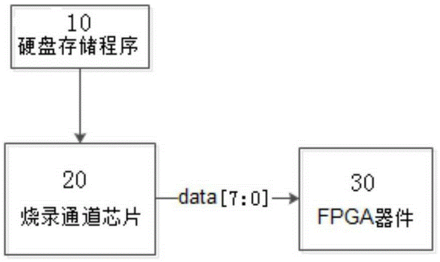
[0018] First refer to figure 1 , which is a structural diagram of an FPGA pin loading device in the prior art. As described in the background technology section, in the FPGA loading method of the prior art, the programming channel chip 20 is used to transmit the program 10 stored inside the hard disk, and the data[7:0] data line is used to transmit the program to the FPGA device 30, In order to complete the data loading or burning. However, as mentioned above, there is a waste of pins in this way.

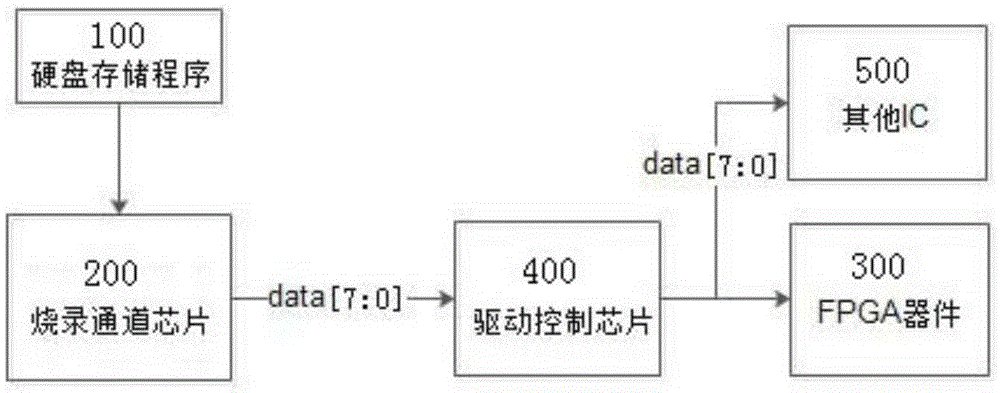
[0019] see below figure 2 , which is a structural diagram of the device for loading and multiplexing FPGA pins according to the present inven...


PUM


Abstract

The invention relates to the communication field, in particular to an FPGA pin loading reuse device and method, and aims to solve the problem that pin waste is caused due to an existing FPGA loading method. The FPGA pin loading reuse device comprises a burn channel chip which is used for receiving a program from a hard disk and burning the received program on to an FPGA and is characterized in that the FPGA pin loading reuse device further comprises a driving control chip which is arranged between the burn channel chip and the FPGA, the driving control chip is used for controlling on and off of burn data lines at two ends of the driving control chip so that a burn pin of the burn channel chip can be reused. According to the technical scheme, the technical staff in the field can understand that a special burn pin can be reused, not only can the loading speed be improved, but also the problem that the pin source is tight is solved to the largest extent.

Description

technical field [0001] The invention relates to the communication field, and specifically provides an FPGA pin loading and multiplexing device and method. Background technique [0002] FPGA (Field Programmable Gate Array), that is, field programmable gate array, is a product of further development on the basis of programmable devices such as PAL, GAL, and CPLD. It emerged as a semi-custom circuit in the field of application-specific integrated circuits (ASIC), which not only solves the shortcomings of custom circuits, but also overcomes the shortcomings of the limited number of original programmable device gates. The circuit design completed in hardware description language (Verilog or VHDL) can be quickly loaded or burned to FPGA for testing after simple synthesis and layout, which is the mainstream of modern IC design verification technology. These editable components can be used to implement some basic logic gates (such as AND, OR, XOR, NOT) or more complex combinational...

Claims


Application Information

Patent Timeline
IPC IPC(8): G06F9/445
Inventor 李竞航汪雷黄少杰
Owner 北京浩瀚深度信息技术股份有限公司
Features
  • R&D
  • Intellectual Property
  • Life Sciences
  • Materials
  • Tech Scout
  • Unparalleled Data Quality
  • Higher Quality Content
  • 60% Fewer Hallucinations
Learn More