A method for repairing silicon wafer defects

A silicon wafer and defect technology, applied in the field of post-processing of solar silicon wafers, can solve problems such as resource and cost waste, difficulty in meeting market demand, etc., and achieve the effect of preventing injury and damage

Active Publication Date: 2017-06-20
江苏美科太阳能科技股份有限公司
View PDF5 Cites 0 Cited by
  • Summary
  • Abstract
  • Description
  • Claims
  • Application Information

AI Technical Summary

Problems solved by technology

[0002] With the increase of human demand for energy, solar silicon wafers have become a new energy source, but the solar silicon wafer wire-cutting processing technology is not 100% qualified, and a small amount of edge defect wafers will be produced during the cutting process. Silicon-like wafers are only slightly inferior to normal silicon wafers in appearance, and other functions are the same as normal silicon wafers. If they are discarded, it will cause a lot of waste of resources and costs. If they are not discarded, it will be difficult to meet market demand.

Method used


Image

  • A method for repairing silicon wafer defects
  • A method for repairing silicon wafer defects

Examples


Embodiment Construction

[0024] The specific embodiment of the present invention will be further described below in conjunction with accompanying drawing:

[0025] A method for repairing silicon wafer defects, the method is as follows:

[0026] (1) Make special tooling

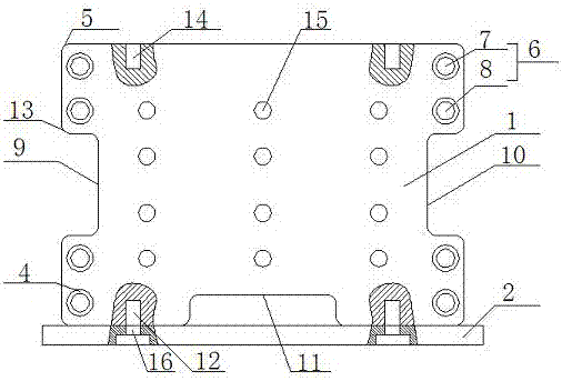
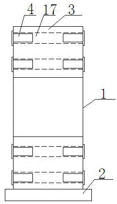
[0027] Make a special tooling for clamping silicon wafers, the special tooling includes a side plate 1, a bottom plate 2, a connecting block 3 and a nut 4, the side plate 1 has two pieces, and the side plate 1 is made of PTFE material. The side plate 1 is a rectangular structure, the four corners of the side plate 1 are all rounded corners 5, and the four corners are provided with a connecting hole group 6, and the connecting hole group 6 includes a first connecting hole 7 and a second connecting hole 8. The side plate Both sides of 1 are provided with a first groove 9 and a second groove 10 respectively, and the first groove 9 and the second groove 10 are arranged coaxially, and both are between two groups of connecting hole groups ...


PUM


Abstract

The invention relates to a novel silicon wafer flaw finishing technology. The technological method includes the following steps: (1) a special tool is manufactured; (2) a silicon wafer is clamped; and (3) polishing is carried out through a grinding wheel, an original flaw part is subject to equipment edge polishing through the grinding wheel under the condition that the size of a silicon wafer is not influenced until the depth is 0.25 mm, no abnormal conditions exist when a user sees the surface of the silicon wafer, only slight grinding cracks can be seen from the lateral face, and no influence is generated on follow-up using of the silicon wafer. By means of machining, the edge flaw part of an original flaw silicon wafer is polished until the grade A product standard of the silicon wafer is met; meanwhile, the original nature of the silicon wafer is not changed, and the appearance flaws of the silicon wafer are repaired with the most direct, simple, convenient and effective method.

Description

technical field [0001] The invention relates to a method for repairing silicon chip defects, which belongs to the field of post-processing of solar silicon chips. Background technique [0002] With the increase of human demand for energy, solar silicon wafers have become a new energy source, but the solar silicon wafer wire-cutting processing technology is not 100% qualified, and a small amount of edge defect wafers will be produced during the cutting process. Silicon-like wafers are only slightly inferior to normal silicon wafers in appearance, and their other functions are the same as normal silicon wafers. If they are discarded, a lot of resources and costs will be wasted, and if they are not discarded, it will be difficult to meet market demand. Contents of the invention [0003] The purpose of the present invention is to provide a method for repairing silicon wafer defects in view of the defects in the prior art. By reprocessing and edging the defective silicon wafers...

Claims


Application Information

Patent Timeline
Patent Type & Authority Patents(China)
IPC IPC(8): B24B9/06B24B41/06
CPCB24B9/065B24B41/06
Inventor 翟彩虹王禄堡陆继波
Owner 江苏美科太阳能科技股份有限公司
Why Eureka
Try Eureka