A pixel unit, its manufacturing method, and display device

A pixel unit and sub-pixel unit technology, applied in the direction of electrical components, semiconductor/solid-state device manufacturing, diodes, etc., can solve the problems of increasing evaporation costs and achieve the effect of improving display life and reducing power consumption

Active Publication Date: 2018-05-22
BOE TECH GRP CO LTD +1
View PDF5 Cites 0 Cited by
  • Summary
  • Abstract
  • Description
  • Claims
  • Application Information

AI Technical Summary

Problems solved by technology

[0004] The purpose of the present invention is to provide a pixel unit, its manufacturing method, and a display device, which are used to solve the problem of increasing the evaporation cost caused by the need to perform multiple evaporations when manufacturing a white sub-pixel unit

Method used


Image

  • A pixel unit, its manufacturing method, and display device
  • A pixel unit, its manufacturing method, and display device
  • A pixel unit, its manufacturing method, and display device

Examples


Embodiment 1

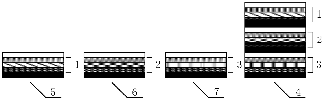
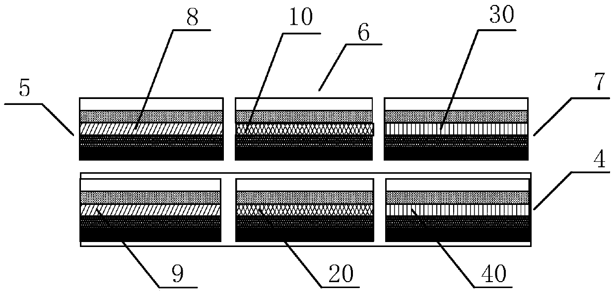
[0061] See Figure 5 , when And When For example, in this case, X R : X G : X B : (W R +W G +W B )=3:3:3:3=1:1:1:1, namely X R =X G =X B =(W R +W G +W B ); Therefore, when the same driving voltage is applied to each sub-pixel unit, the corresponding light brightness of each sub-pixel unit is the same, so that the light-emitting brightness of the pixel unit composed of it is more uniform.

Embodiment 2

[0063] See Image 6 , when 时,X R : X G : X B : (W R +W G +W B )=1:1:1:3, that is In this case, the area of ​​the organic electroluminescent material layer corresponding to the red sub-pixel unit 5, the green sub-pixel unit 6 and the blue sub-pixel unit 7 is equal, and the organic electroluminescent material layer corresponding to the white sub-pixel unit 4 The area is relatively large. Therefore, when the same driving voltage is applied to the red sub-pixel unit 5, the green sub-pixel unit 6 and the blue sub-pixel unit 7, the red sub-pixel unit 5, the green sub-pixel unit 6 and the blue sub-pixel unit The brightness of the light emitted by the pixel unit 7 is the same, and more uniform color display can be realized after mixing these lights; and when the driving voltage is applied to the white sub-pixel unit 4, the brightness of the white light emitted by the white sub-pixel unit 4 is relatively high.

Embodiment 3

[0065] See Figure 7 , when When For example, in this case, X R : X G : X B : (W R +W G +W B )=4:1:1:6. Compared with the case of the first embodiment, the area of ​​the organic electroluminescent material layer corresponding to the white sub-pixel unit 4 is larger. When the driving voltage is applied to the white sub-pixel unit 4, the white The sub-pixel unit 4 can also emit high-brightness white light, and this type of pixel unit can be used in medical equipment to give full play to its high-brightness display effect.


PUM


Abstract

The invention discloses a pixel unit, a manufacturing method thereof, and a display device, and relates to the field of display technology, in order to solve the problem of increasing the evaporation cost caused by multiple times of evaporation when manufacturing a white sub-pixel unit. The white sub-pixel unit in the pixel unit includes: a white light carrier injection layer formed in the same patterning process as the red light carrier injection layer, the green light carrier injection layer and the blue light carrier injection layer, and Red light carrier transport layer, green light carrier transport layer and blue light carrier transport layer are formed in the same patterning process, white light carrier transport layer, organic electroluminescent material layer corresponding to other sub-pixel units A white light organic electroluminescent material layer formed in the same patterning process. The pixel unit provided by the invention is used in OLED display screens.

Description

Technical field [0001] The present invention relates to the field of display technology, in particular to a pixel unit, a manufacturing method thereof, and a display device. Background technique [0002] An organic light-emitting diode (Organic Light-Emitting Diode, hereinafter referred to as OLED) display screen is a display screen composed of an anode, a cathode, and an organic material layer arranged between the anode and the cathode, wherein the organic material layer includes an empty Hole injection layer, hole transport layer, organic electroluminescent material layer, electron transport layer and electron injection layer. During operation, a driving voltage is applied between the anode and cathode of the OLED display screen to inject electrons and holes into the organic electroluminescent material layer through the hole injection layer, hole transport layer, electron transport layer, and electron injection layer. Electrons and holes are recombined in the organic electrolu...

Claims


Application Information

Patent Timeline
Patent Type & Authority Patents(China)
IPC IPC(8): H01L27/32H01L51/56
CPCH10K59/35H10K71/00H10K59/351H10K59/352H10K59/32H10K71/10H10K50/11H10K50/15H10K50/16H10K50/17H10K50/171
Inventor 陈文强
Owner BOE TECH GRP CO LTD
Why Eureka
Try Eureka