Display device, array substrate and manufacturing method thereof

A technology of an array substrate and a manufacturing method, applied in the field of display devices, capable of solving problems such as unevenness, first electrode via hole etching, dark spots of OLED displays, etc., achieving the effect of increasing pattern density and solving dark spots of the display screen

Active Publication Date: 2016-03-09
WUHAN TIANMA MICRO ELECTRONICS CO LTD +1
View PDF4 Cites 6 Cited by
  • Summary
  • Abstract
  • Description
  • Claims
  • Application Information

AI Technical Summary

Problems solved by technology

[0004] In order to solve the above problem, the present invention provides a display device, an array substrate and a manufacturing method thereof, so as to solve defects such as dark spots in the OLED display caused by via holes or uneven etching of the first electrode in the prior art. The problem

Method used


Image

  • Display device, array substrate and manufacturing method thereof
  • Display device, array substrate and manufacturing method thereof
  • Display device, array substrate and manufacturing method thereof

Examples


Embodiment Construction

[0026] The following will clearly and completely describe the technical solutions in the embodiments of the present invention with reference to the accompanying drawings in the embodiments of the present invention. Obviously, the described embodiments are only some, not all, embodiments of the present invention. Based on the embodiments of the present invention, all other embodiments obtained by persons of ordinary skill in the art without making creative efforts belong to the protection scope of the present invention.

[0027] One embodiment of the present invention provides a method for fabricating an array substrate, the array substrate is an array substrate of an OLED display, refer to figure 1 , figure 1 An embodiment of the present invention provides a flowchart of a method for manufacturing an array substrate, and the method for manufacturing an array substrate includes:

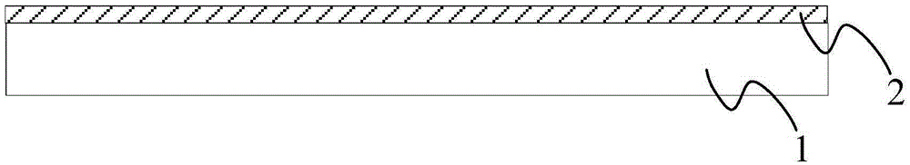
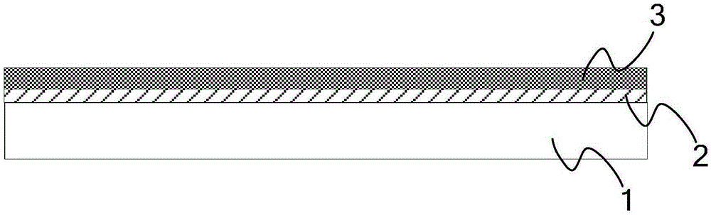
[0028] S101: Provide a substrate, where the substrate includes a substrate and a TFT array locate...


PUM


Abstract

The invention provides a display device, an array substrate and a manufacturing method thereof. The manufacturing method comprises the following steps: providing a substrate, wherein the substrate includes a base and a TFT array disposed on the surface of the base; forming a first electrode layer on the surface of the TFT array of the base; forming a mask on the surface of the first electrode layer, wherein the mask is provided with multiple first electrode patterns and at least one filling pattern disposed between the first electrode patterns; and etching the first electrode layer with the mask to form multiple first electrodes, wherein the first electrode layer covered by the filling patterns is partially or fully etched in the etching process. According to the invention, the pattern density of the first electrode patterns is increased through the filling patterns between the first electrode patterns, and therefore, the problem that the first electrodes are over-etched or etched unevenly in the etching process is avoided, and dark spots and other defects of the display caused thereby are overcome.

Description

technical field [0001] The present invention relates to the technical field of display devices, and more specifically, to an array substrate, a manufacturing method thereof, and a display device including the array substrate. Background technique [0002] Existing OLED (Organic Light-Emitting Diode, organic laser display) display includes a plurality of OLED pixel units, and each OLED pixel unit includes a first electrode, a second electrode and an organic light between the first electrode and the second electrode. The light-emitting layer, wherein the first electrode is an anode, and the second electrode is a cathode. The display device inputs electrons to the organic light-emitting layer through the cathode and absorbs electrons from the organic light-emitting layer through the anode to excite the organic light-emitting layer to emit light. [0003] In the prior art, when making the first electrode, the first electrode layer covering the entire substrate is first formed, a...

Claims


Application Information

Patent Timeline
Patent Type & Authority Applications(China)
IPC IPC(8): H01L27/12H01L27/32H01L21/77
CPCH01L27/1288H10K59/12
Inventor 张鹏李玥周益敏沈洵
Owner WUHAN TIANMA MICRO ELECTRONICS CO LTD
Why Eureka
Try Eureka