Pixel defining structure, manufacturing method for same, display panel and display apparatus

A pixel definition, display panel technology, applied in the direction of optics, instruments, electrical components, etc., can solve problems such as difficult to control independent, difficult to achieve printing and preparation of high-resolution display devices

Inactive Publication Date: 2016-03-16
TCL CORPORATION
View PDF3 Cites 12 Cited by
  • Summary
  • Abstract
  • Description
  • Claims
  • Application Information

AI Technical Summary

Problems solved by technology

If the resolution is further increased, the sub-pixel size will be further reduced, and it will be difficult to control the ink in each sub-pixel to be...

Method used


Image

  • Pixel defining structure, manufacturing method for same, display panel and display apparatus
  • Pixel defining structure, manufacturing method for same, display panel and display apparatus
  • Pixel defining structure, manufacturing method for same, display panel and display apparatus

Examples


Embodiment Construction

[0028] In order to make the object, technical solution and effect of the present invention more clear and definite, the present invention will be further described in detail below. It should be understood that the specific embodiments described here are only used to explain the present invention, not to limit the present invention.

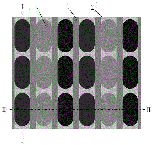
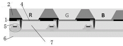
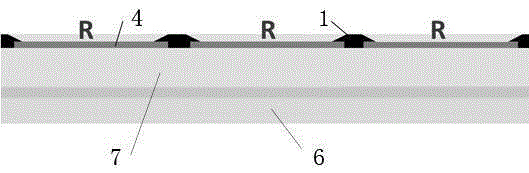
[0029] The present invention provides a structural diagram of a preferred embodiment of a pixel defining structure, such as figure 1 as shown, figure 2 for figure 1 The pixel defines the section view of structure I-I, image 3 for figure 1 The pixels define the section view at structure II-II. 1 represents the first pixel defining layer, 2 represents the second pixel defining layer, 3 represents the sub-pixel, 4 represents the pixel electrode, 5 represents the thin film transistor (ThinFilmTransistor, TFT for short), 6 represents the substrate, and 7 represents the passivation planar layer.

[0030] like figure 1 , figure 2 , image 3 As...


PUM

PropertyMeasurementUnit
Thicknessaaaaaaaaaa
Thicknessaaaaaaaaaa

Abstract

The invention discloses a pixel defining structure, a manufacturing method for the same, a display panel and a display apparatus. The pixel defining structure comprises a first pixel defining layer and a second pixel defining layer arranged on the first pixel defining layer, wherein the pixel defining layer is provided with a plurality of first openings one-to-one corresponding to each sub-pixel illuminating area; and the second defining layer is provided with a plurality of second openings co-used by sub-pixels having the same color. Ink can be prevented from overflowing due to excessive small area of single sub-pixel and size of each sub-pixel can be relatively reduced; effectiveness of printing technology can be guaranteed; ink can be prevented from overflowing due to excessive small area of each sub-pixel during the printing process; and limitation of high-definition display component preparation by the printing technology can be solved, and the printing high-definition display component can be manufactured.

Description

technical field [0001] The present invention relates to the field of organic light-emitting display technology, in particular to a pixel defining structure and manufacturing method, a display panel and a display device. Background technique [0002] The use of solution processing to manufacture OLED and QLED displays is an important direction for the future development of display technology due to its advantages of low cost, high productivity, and easy realization of large sizes. Among them, printing technology is considered to be the most effective way to realize OLED and QLED low-cost and large-area full-color display. [0003] In the printing process, due to the influence of equipment precision and droplet size, for the traditional RGBStripe (RGB strip) arranged pixel structure (such as figure 1 As shown), when the resolution of the display device reaches 200ppi, the width of each sub-pixel will be reduced to 42μm. At the same time, due to the existence of the pixel defi...

Claims


Application Information

Patent Timeline
IPC IPC(8): G02F1/1333G02F1/1343H01L27/32
CPCG02F1/1333G02F1/1343H10K59/122
Inventor 陈亚文
Owner TCL CORPORATION
Why Eureka
Try Eureka