A printed high-resolution display device and its manufacturing method

A technology with high resolution and manufacturing methods, applied in semiconductor/solid-state device manufacturing, electrical solid-state devices, semiconductor devices, etc., can solve the problem that the printing process is difficult to further improve the display resolution, etc., to reduce the area and increase the deposition area Effect

Active Publication Date: 2018-05-08
武汉国创科光电装备有限公司
View PDF3 Cites 0 Cited by
  • Summary
  • Abstract
  • Description
  • Claims
  • Application Information

AI Technical Summary

Problems solved by technology

[0006] In view of the above deficiencies in the prior art, the purpose of the present invention is to provide a printed high-resolution display device and its manufacturing method, aiming to solve the problem that the existing printing process is difficult to further improve the resolution of the display

Method used


Image

  • A printed high-resolution display device and its manufacturing method
  • A printed high-resolution display device and its manufacturing method
  • A printed high-resolution display device and its manufacturing method

Examples


Embodiment 1

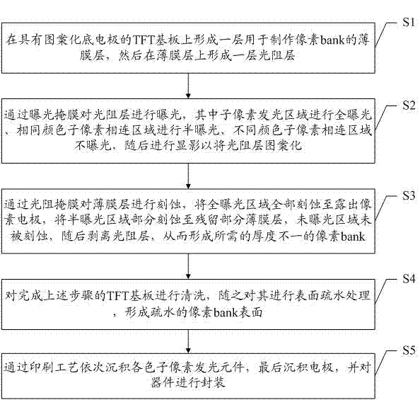
[0036] A method for manufacturing printed high-resolution display devices, combining figure 2 with image 3 As shown, it includes the steps:

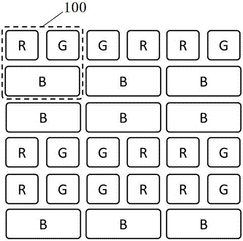
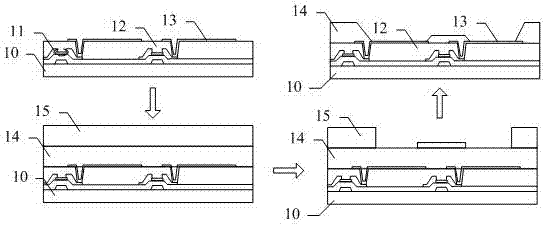
[0037] S1. A thin film layer 14 for making a pixel bank is formed on the TFT substrate 10 with a patterned bottom electrode 13 (there is a TFT array 11, a passivation flat layer 12 and a patterned bottom electrode 13), and then a thin film layer 14 for making a pixel bank is formed on the thin film A photoresist layer 15 is formed on the layer 14;

[0038] S2. Expose the photoresist layer 15 through an exposure mask, where the light-emitting area of ​​the sub-pixels is fully exposed, the connected area of ​​the sub-pixels of the same color is half exposed, and the connected areas of the sub-pixels of different colors are not exposed, and then the photoresist layer is developed. 15 patterning; full exposure is to completely remove the photoresist layer 15, half exposure is to partially remove the photoresist layer 15 to retain a thin layer o...

Embodiment 2

[0045] A method for manufacturing printed high-resolution display devices, combining Figure 4 with Figure 5 As shown, it includes the steps:

[0046] T1. On a TFT substrate 20 with a patterned bottom electrode 23 (in this embodiment, a labeling method different from that in Embodiment 1 is used to distinguish) (there is a TFT array 21, a passivation flat layer 22 and a patterned bottom electrode 23) A photoresist layer 24 for making a pixel bank is formed on it;

[0047] T2. Expose the photoresist layer 24 through the exposure mask, wherein the light-emitting area of ​​the sub-pixels is fully exposed, the connected area of ​​the same color sub-pixels is half exposed, and the connected area of ​​the different color sub-pixels is not exposed;

[0048] T3. Subsequent development processing is performed to completely remove the photoresist layer 24 in the fully exposed area, exposing the patterned bottom electrode 23, partially remove the photoresist layer 24 in the half exposed area, ...


PUM


Abstract

The invention discloses a printing type high-resolution display device and a manufacturing method thereof. In the manufacturing process of the pixel bank, the invention fully exposes the pixel light-emitting area, half-exposes the adjacent areas of the sub-pixels of the same color, and does not expose the connected areas of sub-pixels of different colors. The pixel bank is patterned by etching, developing, etc. , where the pixel bank in the area where sub-pixels of the same color are connected is thinner, defining the sub-pixel light-emitting area, and the bank in the area where sub-pixels of different colors are connected is thicker, defining the ink deposition area in the printing process, thereby doubling the ink deposition area, The area of ​​each sub-pixel can be effectively reduced, combined with the hydrophobic treatment on the surface of the pixel bank, the production of a printed high-resolution display can be realized.

Description

Technical field [0001] The invention relates to the field of display technology, in particular to a printed high-resolution display device and a manufacturing method thereof. Background technique [0002] The method of manufacturing OLED and QLED displays by solution processing is an important direction for the development of future display technology due to its advantages of low cost, high productivity, and easy realization of large sizes. Among them, printing technology is considered to be the most effective way to achieve low-cost and large-area full-color display of OLED and QLED. [0003] In the printing process, due to the impact of equipment accuracy and droplet size, it is difficult to achieve the preparation of high-resolution display devices for the traditional RGB Stripe (RGB stripe) pixel structure. When the resolution of the display device reaches 200 ppi, the width of each sub-pixel will be reduced to 42μm. At the same time, due to the existence of the pixel defining...

Claims


Application Information

Patent Timeline
Patent Type & Authority Patents(China)
IPC IPC(8): H01L51/56H01L27/32
CPCH10K59/35H10K59/122H10K71/13H10K71/00
Inventor 陈亚文
Owner 武汉国创科光电装备有限公司
Why Eureka
Try Eureka