Pixel arrangement structure, light-emitting device and display panel

A technology for pixel arrangement and light-emitting devices, applied in the direction of electric solid devices, semiconductor devices, electrical components, etc., can solve the problem of display resolution limitation, inability to meet high pixel density and other problems

Pending Publication Date: 2020-11-03
GUANGDONG JUHUA PRINTING DISPLAY TECH CO LTD
View PDF5 Cites 0 Cited by
  • Summary
  • Abstract
  • Description
  • Claims
  • Application Information

AI Technical Summary

Problems solved by technology

However, with the continuous development of display technology, the resolution of the display panel is getting higher and higher, and the evaporation method is limited by the accuracy of the shadow mask pattern size, which makes the resolution of the display prepared by this method limited.
To achieve high-resolution products, it is usually necessary to design the pixels to be relatively small, which imposes strict requirements on printing equipment, and current printing equipment cannot meet high-pixel-density printing

Method used


Image

  • Pixel arrangement structure, light-emitting device and display panel
  • Pixel arrangement structure, light-emitting device and display panel
  • Pixel arrangement structure, light-emitting device and display panel

Examples


Embodiment Construction

[0027] In order to facilitate understanding of the present invention, the present invention will be described more fully below, and preferred embodiments of the present invention will be given. However, the present invention may be embodied in many different forms and is not limited to the embodiments described herein. Rather, these embodiments are provided so that a thorough and complete understanding of the present disclosure is provided.

[0028] Unless otherwise defined, all technical and scientific terms used herein have the same meaning as commonly understood by one of ordinary skill in the art to which this invention belongs. The terms used herein in the description of the present invention are for the purpose of describing specific embodiments only, and are not intended to limit the present invention. As used herein, the term "and / or" includes any and all combinations of one or more of the associated listed items.

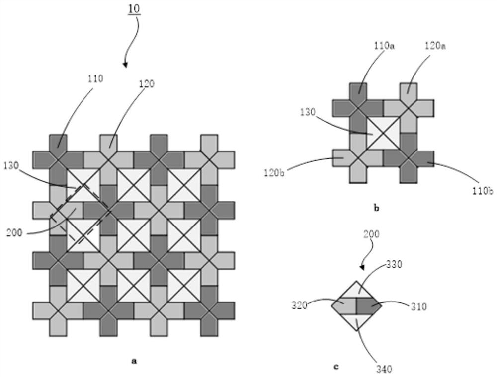
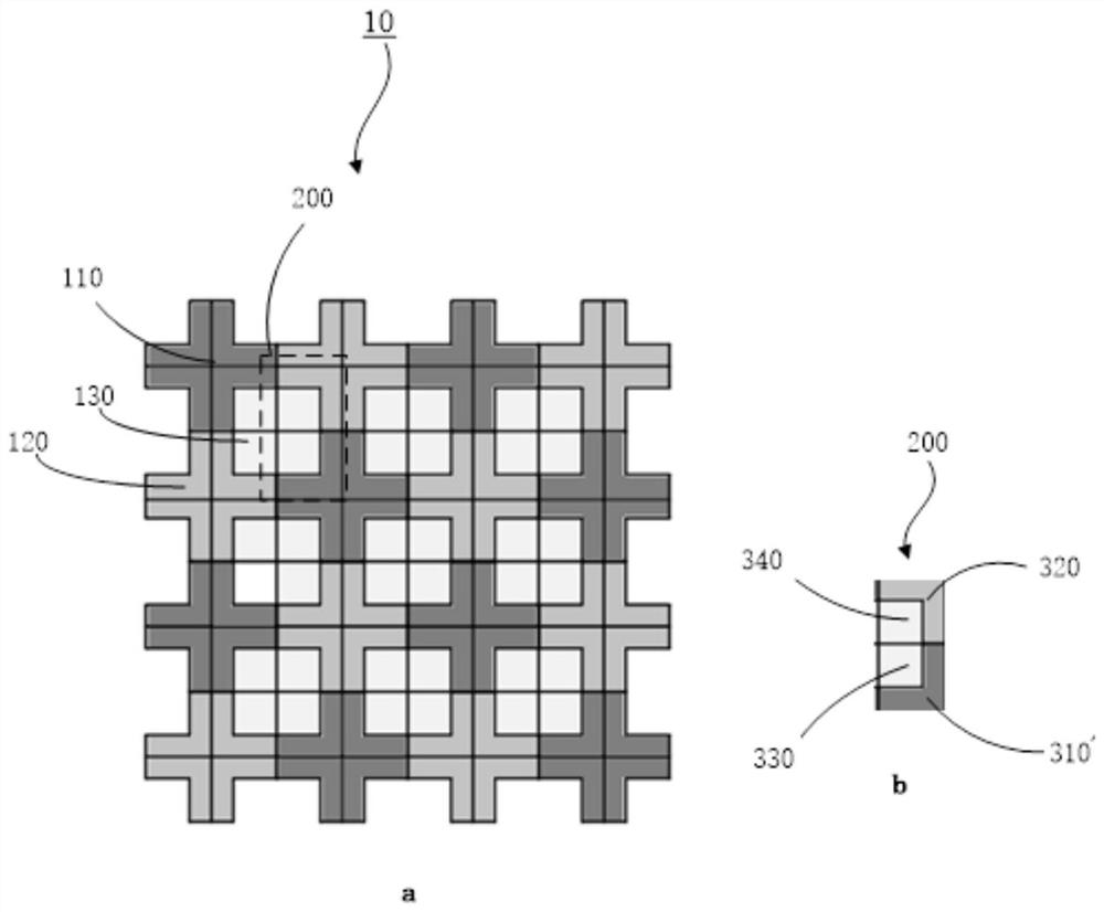
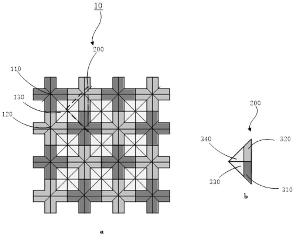
[0029] like Figure 1-Figure 4 As shown, the pixel...


PUM


Abstract

The invention relates to a pixel arrangement structure, a light-emitting device and a display panel. The pixel arrangement structure comprises a plurality of first sub-pixel groups, a plurality of second sub-pixel groups and a plurality of third sub-pixel groups, the first sub-pixel groups, the second sub-pixel groups and the third sub-pixel groups are different in light-emitting color, and each sub-pixel group is composed of a plurality of sub-pixels with the same light-emitting color. The first sub-pixel group and the second sub-pixel group are cross-shaped; the first sub-pixel groups and the second sub-pixel groups which are in a cross shape are alternately arranged in the row direction and the column direction, and every two first sub-pixel groups and every two second sub-pixel groupsare arranged around one third sub-pixel group to form an array structure. According to the pixel arrangement structure, the resolution of the display panel can be improved on the basis of not increasing the preparation difficulty.

Description

technical field [0001] The present invention relates to the technical field of electronic display, in particular to a pixel arrangement structure, a light-emitting device and a display panel. Background technique [0002] At present, OLED displays have the advantages of self-illumination, fast response, wide viewing angle, high brightness, and thinness, and become the mainstream of future displays. The ways to achieve full-color display include vapor deposition of organic light-emitting materials and solution processing. Among them, vapor deposition of organic light-emitting materials is currently the most widely used way to achieve full-color display. It mainly uses precise metal shadow mask and pixel alignment technology to prepare red, green, and blue light-emitting layers by vapor deposition. Solution processing to produce displays, due to its advantages of low cost, high productivity, and easy realization of large sizes, is an important direction for the development of...

Claims


Application Information

Patent Timeline
Patent Type & Authority Applications(China)
IPC IPC(8): H01L27/32
CPCH10K59/353
Inventor 陈亚文史文
Owner GUANGDONG JUHUA PRINTING DISPLAY TECH CO LTD
Why Eureka
Try Eureka