Manufacturing method of multilayer printed circuit board and multilayer printed circuit board

A multi-layer printing and manufacturing method technology, which is applied in the fields of printed circuit manufacturing, multi-layer circuit manufacturing, printed circuit, etc., can solve problems such as the inability to meet the production requirements of multiple lamination high-precision printed circuit boards

Active Publication Date: 2018-05-25
GUANGZHOU FASTPRINT CIRCUIT TECH +2
View PDF3 Cites 0 Cited by
  • Summary
  • Abstract
  • Description
  • Claims
  • Application Information

AI Technical Summary

Problems solved by technology

[0003] The traditional multi-pressing high-precision printed circuit board PIN-LAM (Pin Alignment Lamination Process) manufacturing method, because a set of PIN-LAM slots are used repeatedly for PIN-LAM manufacturing, this method is more common than the common riveting technology. There are certain advantages in the alignment accuracy between layers, but due to the post-lamination process, especially the influence of electroplating / etching on the accuracy of the slot; Accumulation of alignment accuracy errors for times and above has been unable to meet the production requirements of 0.4mm pitch multiple pressing high-precision printed circuit boards

Method used


Image

  • Manufacturing method of multilayer printed circuit board and multilayer printed circuit board
  • Manufacturing method of multilayer printed circuit board and multilayer printed circuit board
  • Manufacturing method of multilayer printed circuit board and multilayer printed circuit board

Examples


Embodiment Construction

[0033] In order to make the object, technical solution and advantages of the present invention clearer, the present invention will be further described in detail below in conjunction with the accompanying drawings and specific implementation methods. It should be understood that the specific embodiments described here are only used to explain the present invention, and do not limit the protection scope of the present invention.

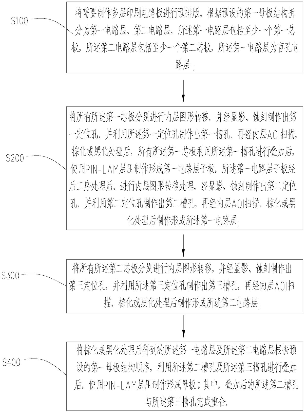
[0034] from figure 1 Shown, the manufacture method of a kind of multilayer printed circuit board of the present invention, comprises steps:

[0035] S100 will need to make a multi-layer printed circuit board for pre-typesetting, and split it into a first circuit layer and a second circuit layer according to the preset first mother board structure, the first circuit layer includes at least one first core board, so The second circuit layer includes at least one second core board, and the first circuit layer is a blind hole circuit layer;

[0036]S200 ...


PUM


Abstract

The invention relates to a manufacturing method for a multi-layer printed circuit board and the multi-layer printed circuit board. The manufacturing method for the multi-layer printed circuit board comprises the following steps of: performing inner layer pattern transfer on all first core boards, forming a first groove hole by utilizing a first positioning hole formed by development, laminating all the first core boards by utilizing the first groove hole to form a first circuit layer sub-board, and forming a second groove hole; and performing inner layer pattern transfer on all second core boards, forming a third groove hole by utilizing a third positioning hole formed by development, performing superposition according to a preset first motherboard structure order, and laminating a first circuit layer and a second circuit layer to form a motherboard. According to the manufacturing method for the multi-layer printed circuit board, the alignment precision of multi-time lamination is improved and the press-fit precision of the multi-layer printed circuit board is enhanced.

Description

technical field [0001] The invention relates to the technical field of multilayer printed circuit boards, in particular to a method for manufacturing a multilayer printed circuit board and the multilayer printed circuit board. Background technique [0002] With the continuous development of electronic products in the direction of multi-function, miniaturization, light weight, and high performance, the requirements for miniaturization and high density of printed circuit boards are also increasing. Its products are also developing from traditional printed boards to high-density laminated printed boards. Interlayer alignment deviation control is an important issue faced by PCB (printed circuit board) manufacturers. To a certain extent, interlayer alignment capability represents the technical level of PCB (printed circuit board) manufacturing technology. Therefore, improving the interlayer alignment capability is of great significance to improving the PCB (printed circuit board...

Claims


Application Information

Patent Timeline
Patent Type & Authority Patents(China)
IPC IPC(8): H05K3/46H05K1/02
CPCH05K1/0298H05K3/4611H05K2203/0537H05K2203/061H05K2203/063
Inventor 徐华胜陈蓓李艳国
Owner GUANGZHOU FASTPRINT CIRCUIT TECH
Why Eureka
Try Eureka