
A high-precision layer-to-layer alignment manufacturing method for a multi-layer circuit board

A technology of a multilayer circuit board and a manufacturing method, which is applied in the direction of multilayer circuit manufacturing, etc., can solve the problems that the alignment accuracy between the layers of the multilayer circuit board cannot meet the production quality requirements and the accuracy error, and avoid multiple punching positions. Influence of precision, effect of improving inter-layer alignment, and reducing inter-layer deviation

Active Publication Date: 2019-12-31
KINWONG ELECTRONICS TECH LONGCHUAN
View PDF5 Cites 0 Cited by
  • Summary
  • Abstract
  • Description
  • Claims
  • Application Information

AI Technical Summary

Problems solved by technology

[0003] The multiple (secondary or above) lamination process of traditional multi-layer circuit boards uses a relatively high-precision PIN-LAM (pin positioning system) manufacturing method. Due to repeated (multiple) use of the same set of PIN-LAM slots for PIN -LAM production, this method has certain technical advantages compared with the conventional riveting process in the alignment accuracy between layers, but due to the process after lamination, especially the influence of electroplating and etching on the graphic size accuracy; The impact of expansion and shrinkage and the accumulation of alignment accuracy errors for the second or more times of lamination lead to the fact that the interlayer alignment accuracy of multi-layer circuit boards in multiple lamination processes cannot meet the production quality requirements

Method used


Image

  • A high-precision layer-to-layer alignment manufacturing method for a multi-layer circuit board
  • A high-precision layer-to-layer alignment manufacturing method for a multi-layer circuit board
  • A high-precision layer-to-layer alignment manufacturing method for a multi-layer circuit board

Examples


Embodiment Construction

[0029] The following specific examples will be used to describe the present invention in detail, and the exemplary embodiments and descriptions of the present invention are used to explain the present invention, but not as a limitation to the present invention.

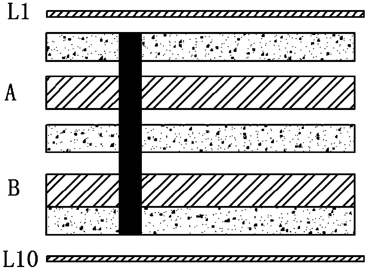
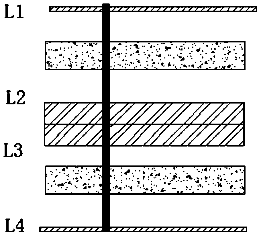
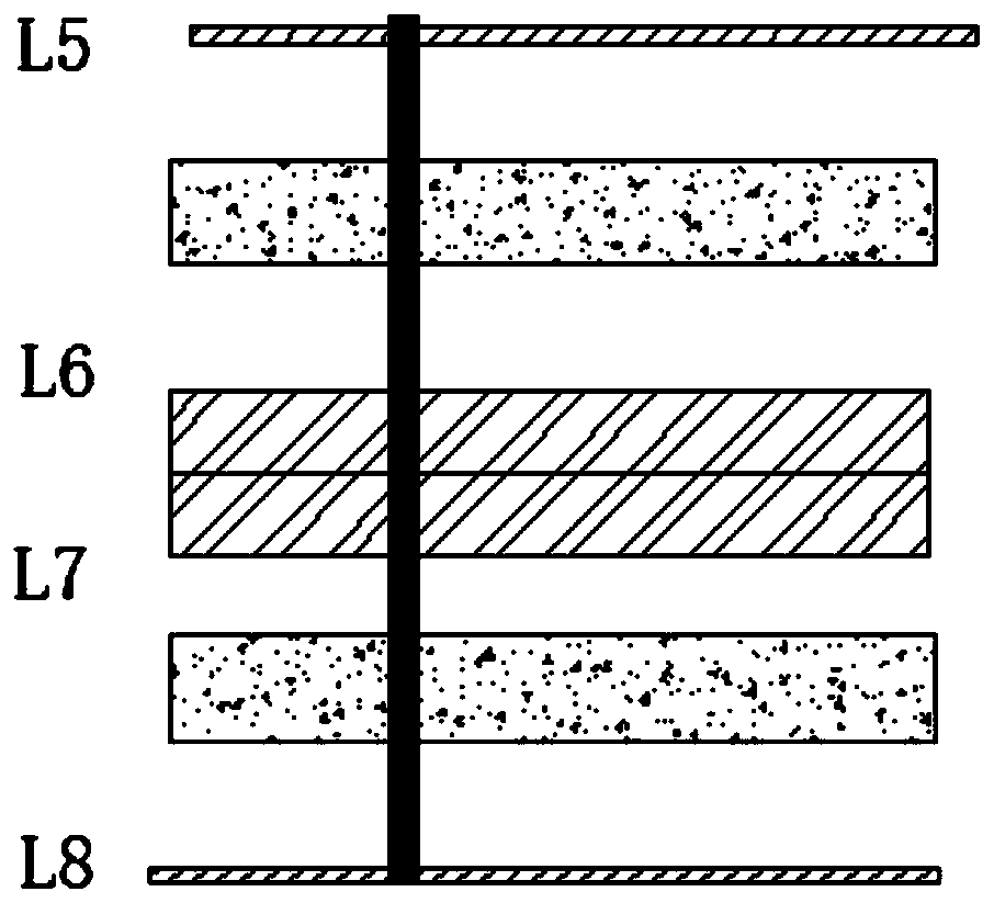
[0030] Such as Figure 1 to Figure 4 As shown, a high-precision layer-to-layer alignment manufacturing method for a multi-layer circuit board,

[0031] (1) It will be necessary to make multi-layer circuit boards for stacking, according to the preset structure of the first sub-board (A board). The structure of the first sub-board (A board) includes at least the first core board (L2 / L3 layer), more than one adhesive sheet, and the outer layer of copper foil (L1 / L4 layer); the first core board is patterned on the inner layer Transfer, develop and etch to make the first layer of CCD fusion positioning block, and then after automatic optical inspection and browning treatment of the inner layer, the first core board is mad...


PUM


Abstract

The present invention discloses a high-precision interlayer registration manufacturing method used for multi-layer circuit boards. The method comprises the following steps: (1) manufacturing a first layer CCD fusion location block on a first structure subsidiary board, and pressing parts of the first structure subsidiary board to form the first structure subsidiary board by using CCD fusion location; (2) manufacturing a second layer CCD fusion location block on a second structure subsidiary board, and pressing the parts of the second structure subsidiary board to form the second structure subsidiary board by using CCD fusion location; (3) and performing CCD fusion location on the first structure subsidiary board, an adhesive sheet, the second structure subsidiary board and outer layer copper foils, pressing the first structure subsidiary board, the adhesive sheet, the second structure subsidiary board and the outer layer copper foils according to a mother board stacking sequence to form a mother board, and completing mother board production after cutting, target-shooting, edge milling and cleaning. The high-precision interlayer registration manufacturing method used for the multi-layer circuit boards has the advantage of scientific and rational design, and the method can effectively avoid position precision influence because a punching machine performs multiple times punching on the multi-layer circuit boards, reduce interlayer deviation between the subsidiary boards, and improve interlayer registration precision and product quality.

Description

technical field [0001] The invention belongs to the technical field of multilayer circuit boards, in particular to an interlayer alignment manufacturing method of multilayer circuit boards. Background technique [0002] With the development of electronic products in the direction of high density, multi-function and high performance, the requirements for the design and manufacturing process of printed circuit boards are getting higher and higher, and its products are also changing from simple structures (double-sided boards, multi-layer boards) to HDI (High-density interconnection board), high-level circuit board (10 layers or above) and other high-end circuit board product development. Interlayer alignment control is a key technical problem faced by PCB (printed circuit board) manufacturers. To a certain extent, interlayer alignment capabilities restrict PCB manufacturers from producing HDI (high-density interconnect boards), high-level board production capacity. Therefore...

Claims


Application Information

Patent Timeline
Patent Type & Authority Patents(China)
IPC IPC(8): H05K3/46
Inventor 谭小林柯勇
Owner KINWONG ELECTRONICS TECH LONGCHUAN
Learn More