Pixel structure and making method thereof, array substrate and display device

A pixel structure and manufacturing method technology, applied in the direction of instruments, nonlinear optics, optics, etc., can solve the problem of reducing storage capacitance and so on

Inactive Publication Date: 2016-04-13
CHONGQING BOE OPTOELECTRONICS +1
View PDF6 Cites 4 Cited by
  • Summary
  • Abstract
  • Description
  • Claims
  • Application Information

AI Technical Summary

Problems solved by technology

[0004] The technical problem to be solved by the present invention is: solve the problem of how to reduce the storage capacitance between the first transparent electrode layer and the second transparent electrode layer in the existing pixel structure

Method used


Image

  • Pixel structure and making method thereof, array substrate and display device
  • Pixel structure and making method thereof, array substrate and display device
  • Pixel structure and making method thereof, array substrate and display device

Examples


Embodiment Construction

[0026] The specific implementation manners of the present invention will be further described in detail below in conjunction with the accompanying drawings and embodiments. The following examples are used to illustrate the present invention, but are not intended to limit the scope of the present invention.

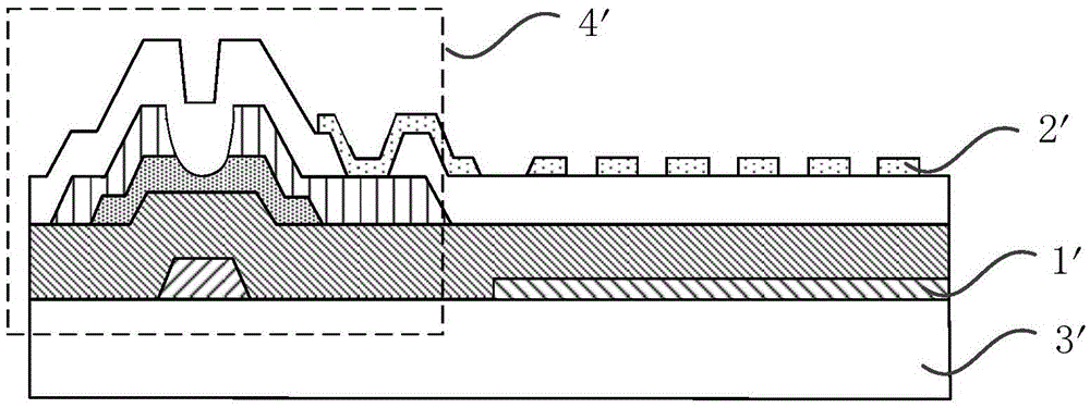
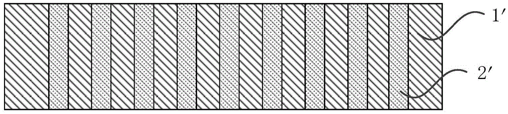
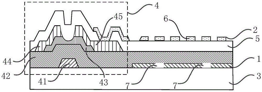
[0027] The present invention provides a pixel structure, including a base substrate and a first transparent electrode layer and a second transparent electrode layer arranged on the base substrate, the second transparent electrode layer includes a plurality of strip electrodes, the first transparent electrode layer At least one slit is included, and each slit is at least partially located within the projection of the strip electrode on the base substrate.

[0028] In the pixel structure provided by the present invention, by forming slits on the first transparent electrode layer and making the slits at least partly located within the projection of the strip electrodes on the...


PUM


Abstract

The invention relates to the technical field of display, and discloses a pixel structure and a making method thereof, an array substrate and a display device. The pixel structure comprises a substrate and a first transparent electrode layer and a second transparent electrode layer which are arranged on the substrate, the second transparent electrode layer comprises multiple strip-shaped electrodes, the first transparent electrode layer comprises at least one slit, and each slit is at least partially located in a projection of the corresponding the strip-shaped electrode in the substrate. According to the pixel structure, by means of the slits formed in the first transparent electrode layer, the overlapping regions of the first transparent electrode layer and the second transparent electrode layer is effectively decreased, storage capacitance formed between the overlapping regions is decreased, and the charging efficiency of pixels and the display quality of the display device are improved.

Description

technical field [0001] The present invention relates to the field of display technology, in particular to a pixel structure and a manufacturing method thereof, an array substrate and a display device. Background technique [0002] The liquid crystal display device is currently the most widely used flat panel display device, which can provide high-resolution color screens for various electronic devices such as mobile phones, personal digital assistants (PDAs), digital cameras, and computers. Among them, the FFS (Fringe Field Switching, fringe field switching technology) liquid crystal display device is favored by the majority of users for its wide viewing angle and high aperture ratio. The FFS liquid crystal display device commonly used at present generally includes a color filter substrate, an array substrate, and a liquid crystal layer arranged between the color filter substrate and the array substrate. Wherein the array substrate is provided with a plurality of data lines...

Claims


Application Information

Patent Timeline
Patent Type & Authority Applications(China)
IPC IPC(8): G02F1/1343
CPCG02F1/134309
Inventor 杨海刚朴正淏李哲胡竞勇
Owner CHONGQING BOE OPTOELECTRONICS
Why Eureka
Try Eureka