Manufacturing method for printed circuit board

A technology of printed circuit boards and manufacturing methods, which is applied in the direction of printed circuit manufacturing, printed circuits, electrical components, etc., can solve the problem of high scrapping cost of design units, and achieve the effect of reducing scrapping costs

Active Publication Date: 2016-04-20
NEW FOUNDER HLDG DEV LLC +1
View PDF5 Cites 7 Cited by
  • Summary
  • Abstract
  • Description
  • Claims
  • Application Information

AI Technical Summary

Problems solved by technology

[0005] Therefore, the technical problem to be solved by the present invention is to overcome the high cost of scrapping badly designed units in the jigsaw printed circuit board in the prior art

Method used


Image

  • Manufacturing method for printed circuit board
  • Manufacturing method for printed circuit board

Examples


Embodiment 1

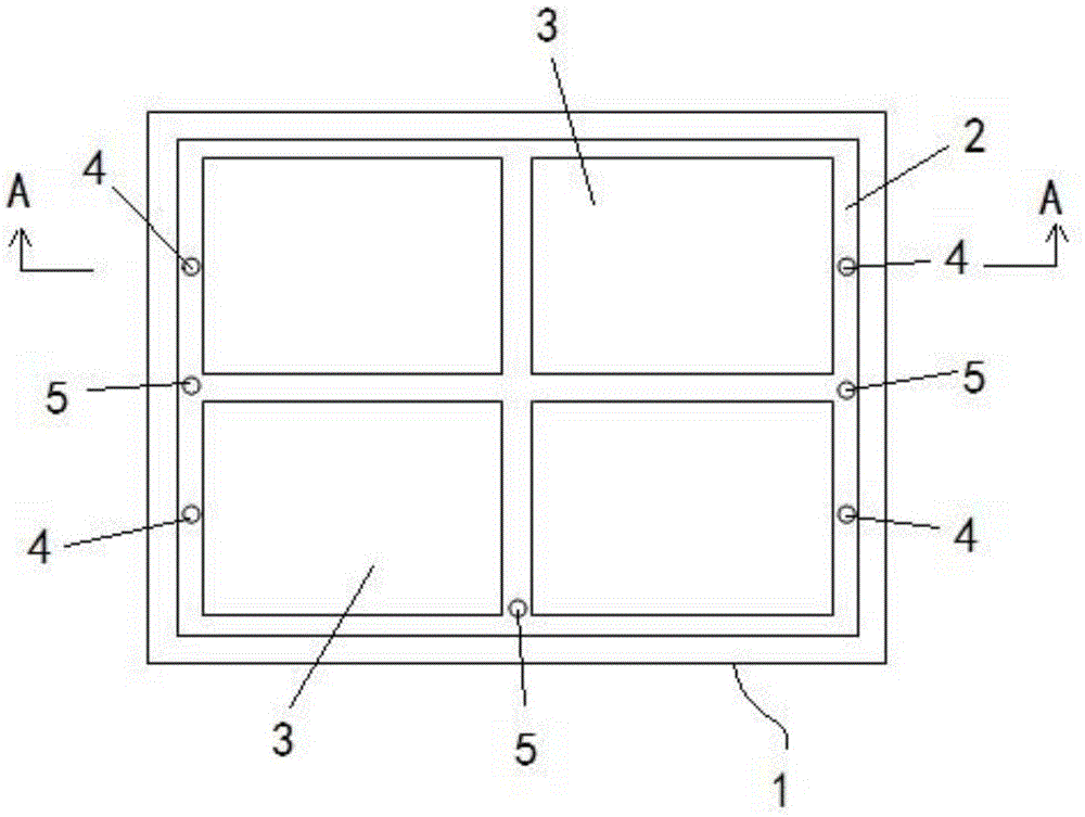
[0032] The present embodiment provides a kind of manufacturing method of printed circuit board, refer to figure 1 with figure 2 shown, including the following steps:

[0033] S1. Form alignment holes 4 on non-working areas of each design unit 3 located on the jigsaw printed circuit board;

[0034] S2. Carry out quality inspection on the design unit 3. For the design unit 3 detected as a defective product, cover the alignment hole 4 corresponding to it to make it opaque, and for the design unit 3 detected as a good product, do not place it with it The corresponding alignment hole 4 is covered and blocked;

[0035] S3. Perform alignment exposure on the jigsaw printed circuit board. When a certain alignment hole 4 is detected to transmit light, perform normal exposure to the design unit 3 corresponding to the alignment hole 4. When a certain alignment hole 4 is detected When the alignment hole 4 is opaque, expose the design unit 3 corresponding to the alignment hole 4 without...

Embodiment 2

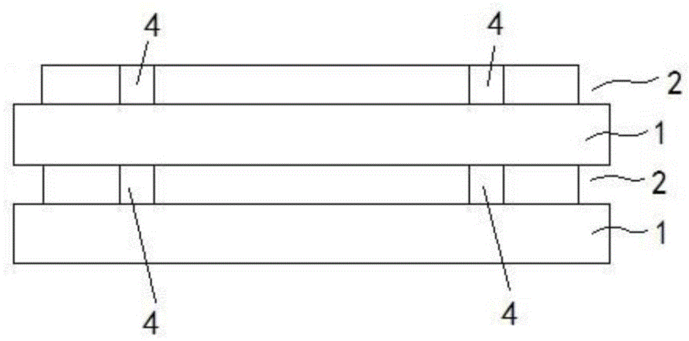
[0044] The present embodiment provides a kind of manufacturing method of printed circuit board, refer to figure 1 with figure 2 shown, including the following steps:

[0045] S1. Form alignment holes 4 on non-working areas of each design unit 3 located on the jigsaw printed circuit board;

[0046] S2. Carry out quality inspection on the design unit 3. For the design unit 3 detected as a defective product, cover the alignment hole 4 corresponding to it to make it opaque, and for the design unit 3 detected as a good product, do not place it with it The corresponding alignment hole 4 is covered and blocked;

[0047] S3. Continue to stack the jigsaw printed circuit boards on the jigsaw printed circuit boards, repeat steps S1 and S2 for the jigsaw printed circuit boards of each layer, and make the jigsaw printed circuit boards arranged on different jigsaw printed circuit boards The positions of the alignment holes (4) coincide until the target number of layers is reached;

[0...


PUM


Abstract

The invention provides a manufacturing method for a printed circuit board. The method comprises: S1, alignment holes are formed in non-working areas of all design units on a jointed printed circuit board; S2, quality detection is carried out on the design unit; if defective product existence is detected, one alignment hole corresponding to the defective product is covered and shielded to prevent light transmission; if good product existence is detected, one alignment hole corresponding to the good product is not covered and shielded; S3, alignment exposure is carried out on the jointed printed circuit board; when light transmission of the alignment hole corresponding to one certain design unit is detected, the design unit is exposed normally; and when no light transmission of alignment hole is detected, the design unit is processed by no-shield exposure; and S4, the manufactured jointed printed circuit board is segmented to obtain a printed circuit board. The design unit processed by normal exposure can be plated with nickel and gold; and the design unit processed by no-shield exposure can not be plated with nickel and gold. Therefore, manufacturing of the good product design unit can be guaranteed and the scrap cost of the defective product design unit can be reduced.

Description

technical field [0001] The invention relates to the technical field of electronic circuits, in particular to a method for manufacturing a printed circuit board. Background technique [0002] With the continuous development and maturity of printed circuit board technology, the imposition design ability of printed circuit board has been continuously improved. In order to improve production efficiency, jigsaw printed circuit boards began to appear in the process of making printed circuit boards. Jigsaw printed circuit board refers to designing multiple independent units on a whole board. The whole board is made together during production. After the production is completed, the whole board is cut, and each unit cut becomes independent. printed circuit board products. [0003] In the prior art, the production of printed circuit board products by splicing printed circuit boards generally includes the following steps: that is, continuous stacking of multiple layers of metal foil ...

Claims


Application Information

Patent Timeline
Patent Type & Authority Applications(China)
IPC IPC(8): H05K3/00
CPCH05K3/0052H05K2203/163
Inventor 车世民陈子形王细心汪汇东
Owner NEW FOUNDER HLDG DEV LLC
Why Eureka
Try Eureka