A secondary etching double-sided circuit board structure and its production process

A double-sided circuit board and secondary etching technology, which is applied to printed circuits, printed circuit manufacturing, electrical components, etc., can solve the problems of uncontrolled product quality, long cycle time, and large cost investment, and simplify the production process. The effect of reducing the difficulty of the job, reducing the cost of PCB production, and reducing the input of human resources

Active Publication Date: 2018-07-10
苏州市三生电子有限公司
View PDF6 Cites 0 Cited by
  • Summary
  • Abstract
  • Description
  • Claims
  • Application Information

AI Technical Summary

Problems solved by technology

[0002] In the current circuit board production process, double-sided circuit boards with GTL circuit layer, GBL internal circuit layer and GBL external circuit layer are all manufactured three times, and the circuit production is completed one by one. The cumulative error of production is very large, and the product quality is not good. When it comes to management and control, the operation cycle is long, the production cycle is long, the production delivery time cannot be improved, and the cost investment is also large, which cannot meet the customer's requirements; after the research, the operation can be completed in the second time, and the product quality can also be improved. be regulated

Method used


Image

  • A secondary etching double-sided circuit board structure and its production process
  • A secondary etching double-sided circuit board structure and its production process
  • A secondary etching double-sided circuit board structure and its production process

Examples


Embodiment Construction

[0027] Below in conjunction with accompanying drawing and embodiment the present invention is described in further detail:

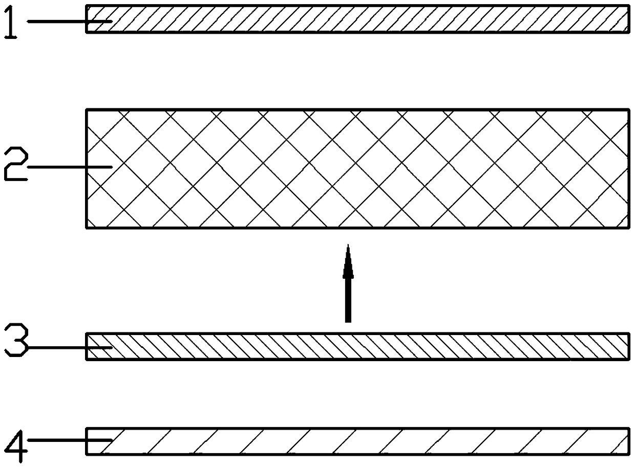
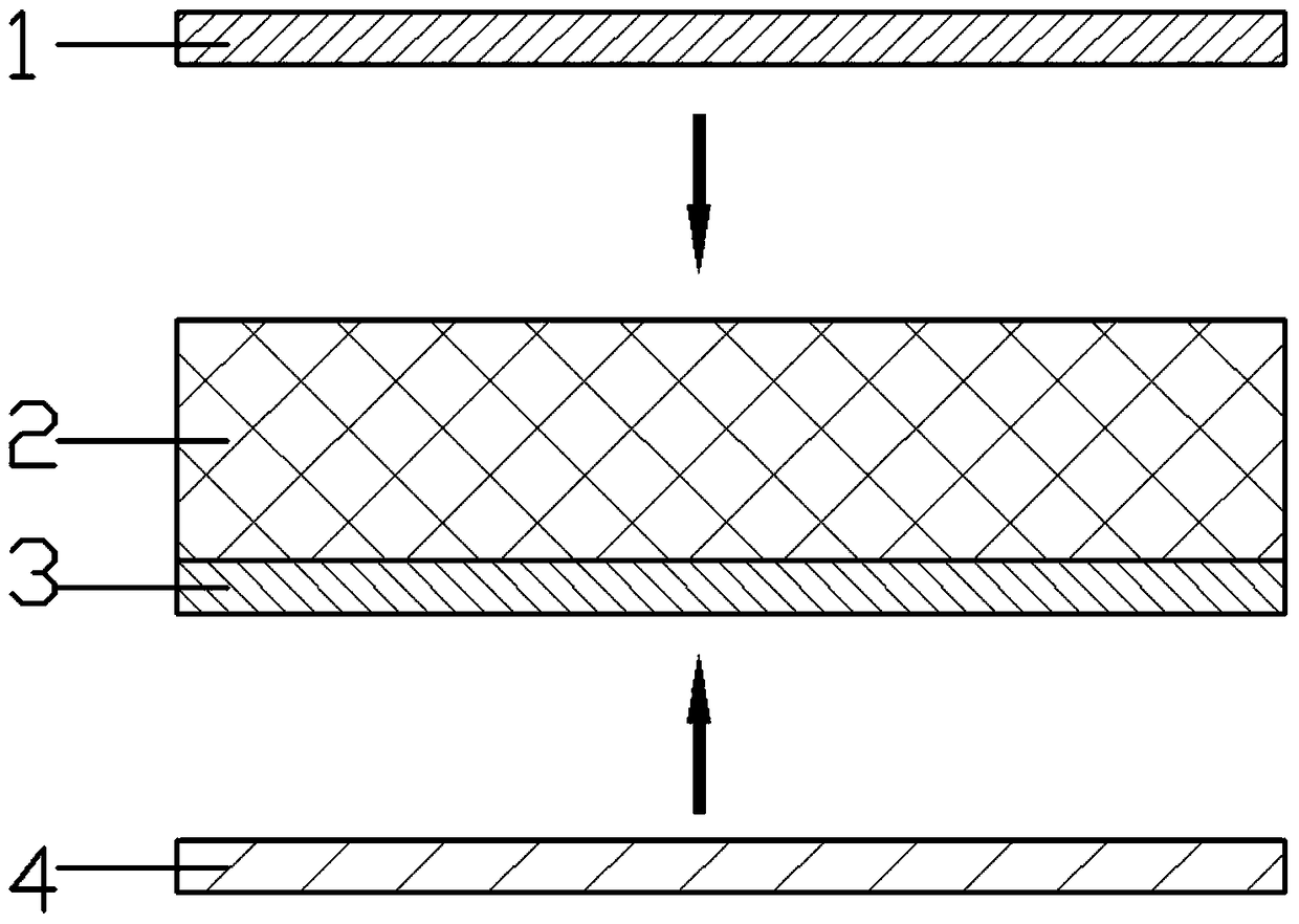
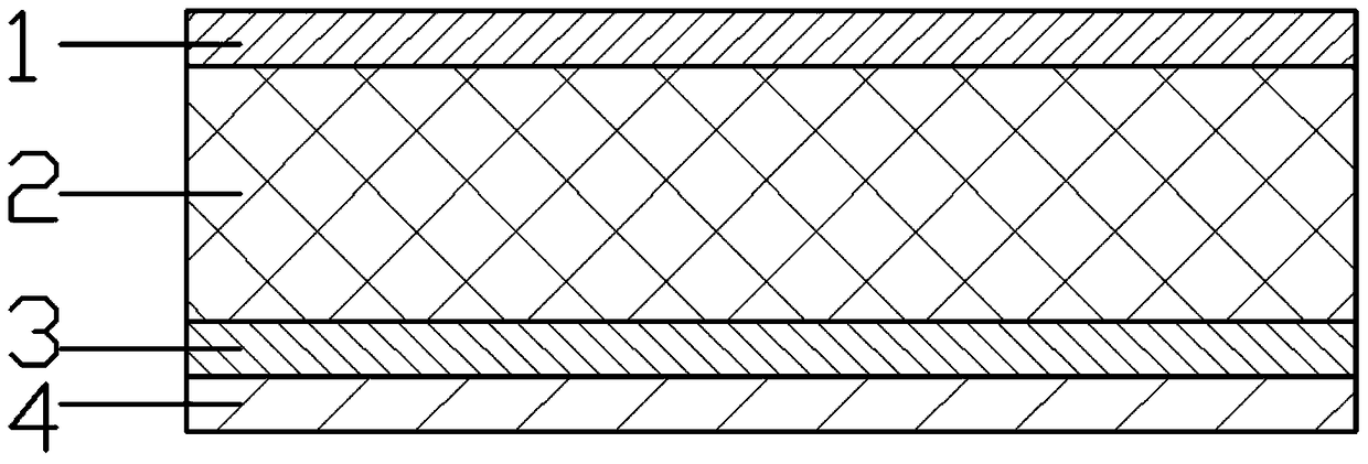
[0028] like image 3 As shown, a secondary etching double-sided circuit board structure includes: GTL line layer 1, insulating PP layer 2 and GBL step surface line layer, characterized in that: the GBL step surface line layer is composed of GBL inner line layer 3 and The GBL outer line layer 4 is formed, the insulating PP layer 2 is located between the GTL line layer 1 and the GBL inner line layer 3, the GBL outer line layer 4 is located on the other side of the GBL inner line layer 3, and the GBL outer line layer 4 is similar to the appearance shape of the GBL inner circuit layer 3, but the size B1 of the GBL inner circuit layer 3 is larger than the size B2 of the GBL outer circuit layer 4, and the size relationship is preferably: B1=B2+0.05mm. The production process of etching double-sided circuit boards includes the sub-process of the first circuit p...


PUM


Abstract

The invention discloses a secondary etching double-sided circuit board structure and its production process. The double-sided circuit board structure of the invention comprises: a GTL circuit layer, an insulating PP layer and a GBL step surface circuit layer, and the GBL step surface circuit layer It is composed of GBL inner line layer and GBL outer line layer, the insulating PP layer is located between the GTL line layer and the GBL inner line layer, the GBL outer line layer is located on the other side of the GBL inner line layer, a secondary etching double The surface circuit board production process includes the following steps: the first circuit production - - - line development cam compensation - - - line inspection - - - etching - - - the second circuit production - - - line development cam compensation - - - circuit Inspection--etching--electrical open and short circuit--after process. The invention only needs secondary production, requires less investment, simplifies the production process and operation difficulty, improves the production efficiency, reduces the production cost, reduces the defective rate of products, and shortens the production cycle of products.

Description

technical field [0001] The invention relates to a circuit board production process, in particular to a secondary etching double-sided circuit board production process. Background technique [0002] In the current circuit board production process, double-sided circuit boards with GTL circuit layer, GBL internal circuit layer and GBL external circuit layer are all manufactured three times, and the circuit production is completed one by one. The cumulative error of production is very large, and the product quality is not good. When it comes to management and control, the operation cycle is long, the production cycle is long, the production delivery time cannot be improved, and the cost investment is also large, which cannot meet the customer's requirements; after the research, the operation can be completed in the second time, and the product quality can also be improved. get regulated. In order to solve the above problems, a new type of superimposed circuit board circuit prod...

Claims


Application Information

Patent Timeline
Patent Type & Authority Patents(China)
IPC IPC(8): H05K3/00
Inventor 孙祥根
Owner 苏州市三生电子有限公司
Why Eureka
Try Eureka