
A method to eliminate the first ten effect of flash annealing machine

An annealing and effect technology, applied in the manufacture of electrical components, semiconductor/solid-state devices, circuits, etc., can solve the problems of waste of production capacity and human resources, increase of production costs, etc., and achieve the goals of avoiding waste, improving product yield, and stabilizing the process environment Effect

Active Publication Date: 2018-03-30
SHANGHAI HUALI MICROELECTRONICS CORP
View PDF5 Cites 0 Cited by
  • Summary
  • Abstract
  • Description
  • Claims
  • Application Information

AI Technical Summary

Problems solved by technology

[0008] The present invention aims at providing a method for eliminating the effect of the first ten pieces of the flash annealing machine in the prior art.

Method used


Image

  • A method to eliminate the first ten effect of flash annealing machine
  • A method to eliminate the first ten effect of flash annealing machine

Examples


Embodiment Construction

[0027] In order to illustrate the technical content, structural features, achieved goals and effects of the present invention in detail, the following will be described in detail in conjunction with the embodiments and accompanying drawings.

[0028] After the traditional ion implantation process, an annealing process is usually used to activate the impurities and repair the damage caused by the ion implantation to the substrate wafer. However, as the feature size of silicon-based devices is reduced to 40 / 28 nanometers, the integration and complexity are enhanced, especially the ultra-shallow junction has stricter control over the diffusion of dopant elements, and only traditional uniform temperature annealing (second level) And the peak annealing (about 1000 milliseconds) can no longer meet the requirements of thermal budget (Thermal Budget), thus affecting the performance of CMOS devices.

[0029] In order to reduce the diffusion of impurities while activating them, more adv...


PUM


Abstract

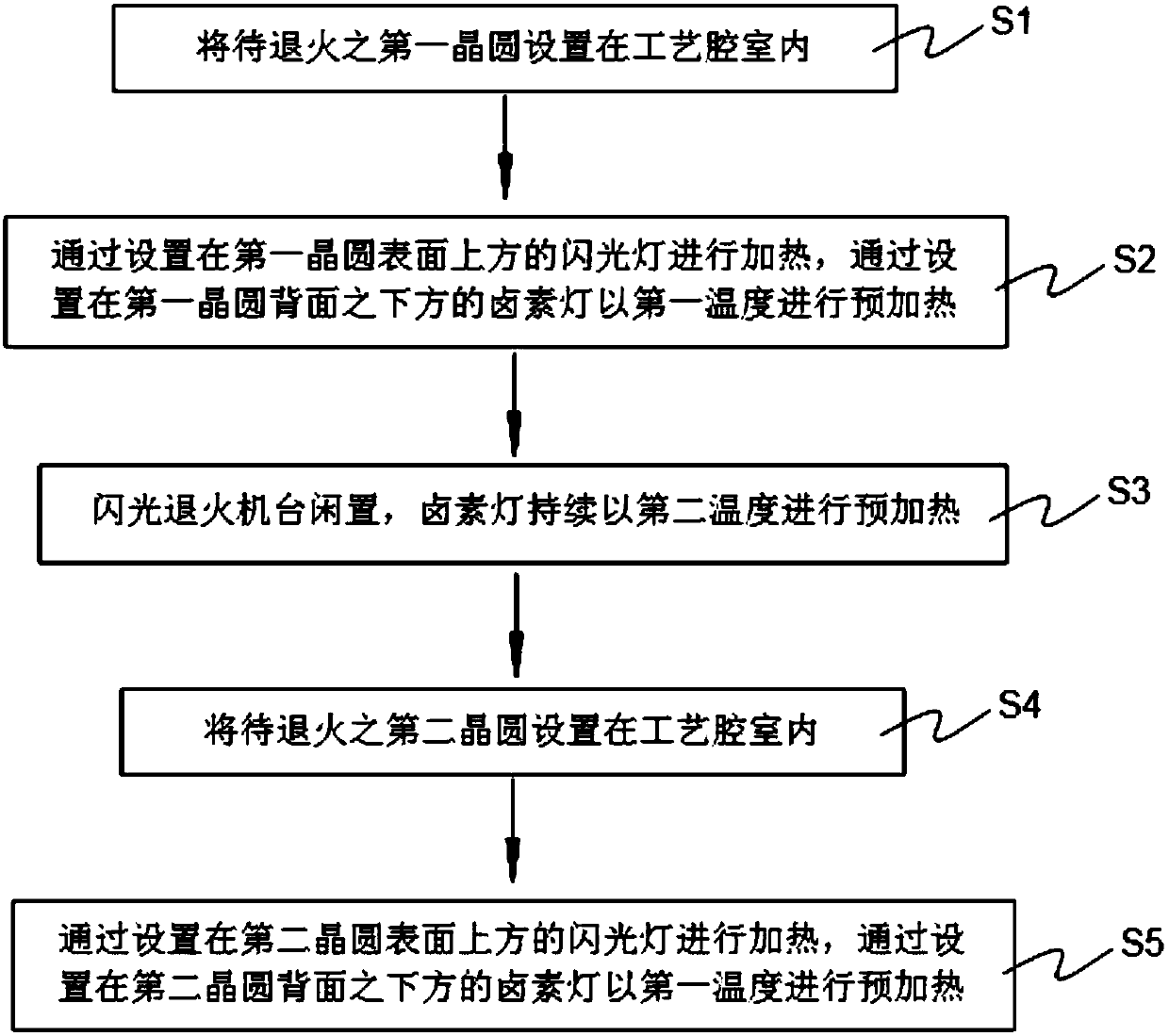
The invention discloses a method for eliminating the first ten-wafer effect of a flash annealing machine. The method comprises the following steps: S1, arranging a first wafer into a process chamber; S2, heating the first wafer via a flashlight above, and preheating the first wafer at a first temperature via a halogen lamp below; S3, idling the flash annealing machine, and continuously preheating the first wafer at a second temperature via the halogen lamp; S4, arranging a second wafer into the process chamber; and S5, heating the second wafer via the flashlight above, and preheating the second wafer at the first temperature via the halogen lamp below. According to the method, when the flash annealing machine is idle, the halogen lamp is continuously adopted for preheating at the second temperature, and the energy generated by the second temperature of preheating is 50-100% of the energy generated by preheating the second wafer with the halogen lamp at the first temperature, so that the process environment in the chamber can be stabilized, the product yield can be improved and the waste of human resources can be avoided.

Description

technical field [0001] The invention relates to the technical field of semiconductor manufacturing, in particular to a method for eliminating the first-ten-piece effect of a flash annealing machine. Background technique [0002] After the traditional ion implantation process, an annealing process is usually used to activate the impurities and repair the damage caused by the ion implantation to the substrate wafer. However, as the feature size of silicon-based devices is reduced to 40 / 28 nanometers, the integration and complexity are enhanced, especially the ultra-shallow junction has stricter control over the diffusion of dopant elements, and only traditional uniform temperature annealing (second level) And the peak annealing (about 1000 milliseconds) can no longer meet the requirements of thermal budget (Thermal Budget), thus affecting the performance of CMOS devices. [0003] In order to reduce the diffusion of impurities while activating them, more advanced annealing tec...

Claims


Application Information

Patent Timeline
Patent Type & Authority Patents(China)
IPC IPC(8): H01L21/67
CPCH01L21/67115
Inventor 邱裕明肖天金余德钦
Owner SHANGHAI HUALI MICROELECTRONICS CORP
Learn More