Image acquisition apparatus, electronic device, and manufacturing method of electronic device

An image acquisition device and technology of electronic equipment, applied in the field of electronics, can solve problems such as low picture definition, and achieve the effects of improving imaging definition, increasing screen ratio, and reducing borders

Active Publication Date: 2016-06-01
LENOVO (BEIJING) CO LTD
View PDF5 Cites 14 Cited by
  • Summary
  • Abstract
  • Description
  • Claims
  • Application Information

AI Technical Summary

Problems solved by technology

[0004] Embodiments of the present invention provide an image acquisition device, an electronic device, and a manufacturing method of the electronic device, which are used to solve the technical problem of low image definition caused by the use of a common wafer-level camera in the prior art

Method used


Image

  • Image acquisition apparatus, electronic device, and manufacturing method of electronic device
  • Image acquisition apparatus, electronic device, and manufacturing method of electronic device
  • Image acquisition apparatus, electronic device, and manufacturing method of electronic device

Examples


Embodiment 1

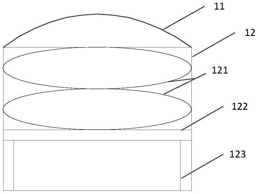
[0056] Please refer to figure 1 , is a cross-sectional view of an image acquisition device provided in Embodiment 1 of the present application, including:

[0057] The wafer-level camera 12, the outer lens 11, the outer lens 11 overlaps the lens of the wafer-level camera 12, and the optical axis of the lens 121 of the wafer-level camera coincides with the optical axis of the outer lens 11, wherein the outer lens 11 can Converging the light reflected by the shooting object, so that the converging light passes through the lens 121 and the infrared filter 122 of the wafer-level camera and reaches the image sensor 123 of the wafer-level camera to generate a first image.

[0058] Optionally, the material of the outer lens 11 is a hard light-transmitting material.

[0059] In a specific embodiment, the outer lens 11 is a hard light-transmitting material, such as quartz glass, sapphire, resin material or synthetic glass, which can be determined according to the actual situation, whi...

Embodiment 2

[0063] Please refer to figure 1 , is a cross-sectional view of an image acquisition device provided in Embodiment 2 of the present application; figure 2 , is a structural diagram of an electronic device provided in this application.

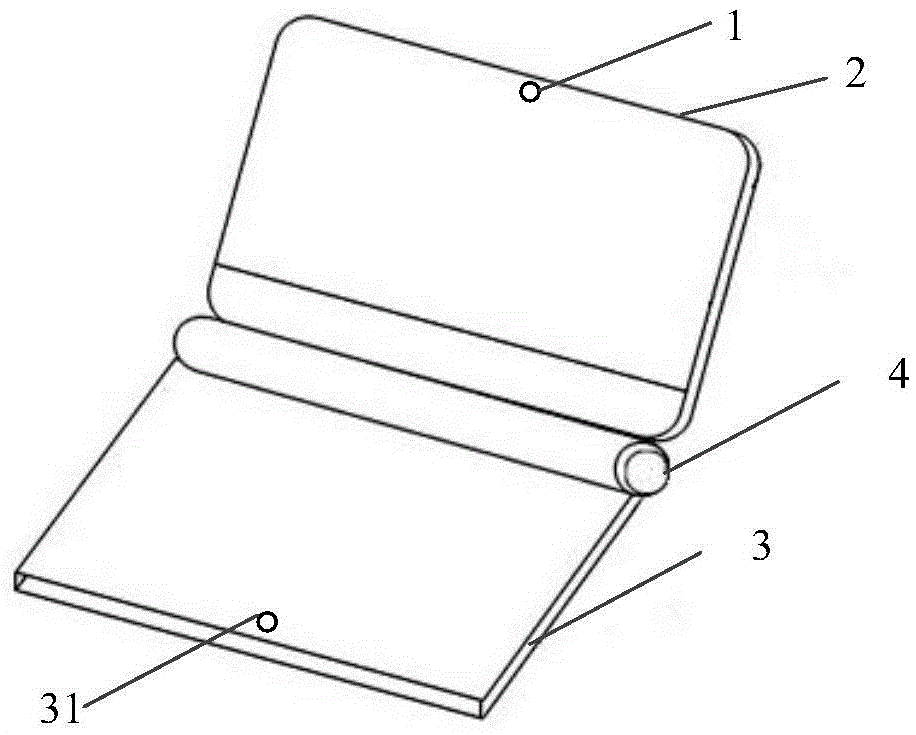
[0064] Based on the same inventive concept as the first embodiment of the present application, the second embodiment of the present application also provides an electronic device, including:

[0065] first ontology 2;

[0066] Second body 3;

[0067] A connection device 4, the connection device 4 connects the first body 2 to the second body 3, wherein the angle value between the first body 2 and the second body 3 can be passed around the The connecting device 4 rotates to change;

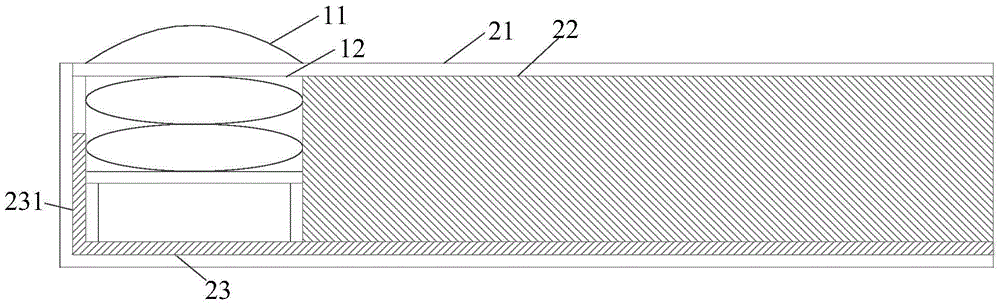
[0068] An image acquisition device 1, the image acquisition device 1 is arranged on the frame of the first body 2, and includes a wafer-level camera 12 and an outer lens 11, wherein the outer lens 11 overlaps the wafer-level camera above the lens 121, and the opt...

Embodiment 3

[0084] Please refer to Figure 4 , the embodiment of the present application provides a method for manufacturing an electronic device, the method comprising:

[0085] S101: Connect the first body to the second body through a connecting device, wherein the angle value between the first body and the second body can be changed by rotating around the connecting device;

[0086] S102: Set the image acquisition device on the frame of the first body, wherein the image acquisition device includes a wafer-level camera and an outer lens, wherein the outer lens overlaps the lens of the wafer-level camera , and the optical axis of the lens of the wafer-level camera coincides with the optical axis of the outer lens; the outer lens can gather the light reflected by the subject, so that the gathered light passes through the lens of the wafer-level camera, The infrared filter reaches the image sensor of the wafer-level camera to generate a first image.

[0087] In a specific embodiment, the...


PUM


Abstract

The invention discloses an image acquisition apparatus, an electronic device, and a manufacturing method of the electronic device. The image acquisition apparatus includes: a wafer-grade pick-up head and an outer lens, wherein the outer lens is overlapped above a lens of the wafer-grade pick-up head; an optical axis of the lens of the wafer-grade pick-up head is coincided with that of the outer lens; and the outer lens can gather the light reflected by a shooting object, so that the gathered light can reach an image sensor of the wafer-grade pick-up head through the lens of the wafer-grade pick-up head and an infrared optical filter to generate a first image.

Description

technical field [0001] The invention relates to the field of electronic technology, in particular to an image acquisition device, electronic equipment and a manufacturing method of the electronic equipment. Background technique [0002] With the continuous development of science and technology, electronic equipment has also been developed rapidly. The design of the display screen of the electronic equipment is getting larger and larger, and the design of the frame is getting narrower and narrower. [0003] In the prior art, a narrow-frame notebook collects video images by using a wafer-level camera. However, in the process of realizing the technical solution of the invention in the embodiment of the present application, the inventor of the present application found that the above-mentioned technology has at least the following technical problems: in the prior art, the camera in the narrow-frame notebook is designed to be very narrow due to the narrow frame design, and the th...

Claims


Application Information

Patent Timeline
Patent Type & Authority Applications(China)
IPC IPC(8): H04N5/225
CPCH04N23/51H04N23/57H04N23/55H04N23/54
Inventor 于宙王智虎
Owner LENOVO (BEIJING) CO LTD
Why Eureka
Try Eureka