
Image processing method, device thereof, and display device

A display device and image processing technology, applied in static indicators, instruments, etc., can solve the problems of reduced display effect, large brightness difference, gray scale difference, etc.

Active Publication Date: 2016-07-06
BOE TECH GRP CO LTD +1
View PDF8 Cites 28 Cited by
  • Summary
  • Abstract
  • Description
  • Claims
  • Application Information

AI Technical Summary

Problems solved by technology

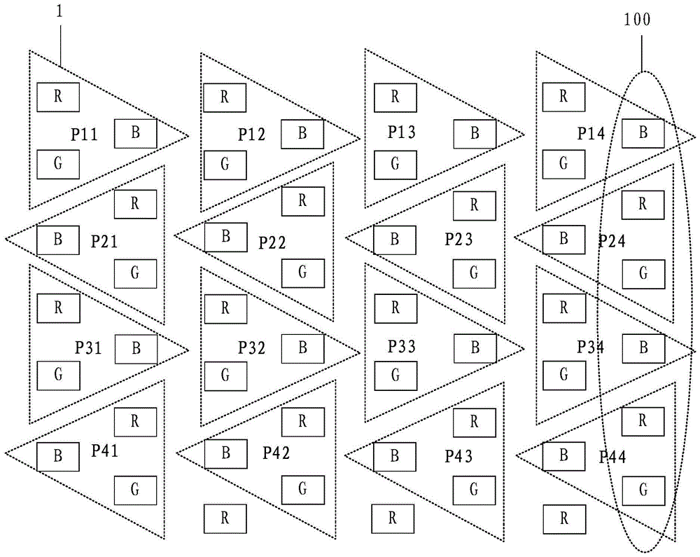
but refer to figure 1 As shown, in a column of sub-pixels 100 located on the outermost side of the edge, each sub-pixel belongs to a different pixel. In this way, when a non-solid color picture is displayed, there is a difference in the gray scale of adjacent sub-pixels, and at the same time, due to the blue sub-pixel The brightness is smaller than that of the red sub-pixel and the green sub-pixel, which further exacerbates the difference in brightness between adjacent sub-pixels, and the sub-pixel 100 in this column is prone to aliasing and color shift, thereby reducing the display effect
example, figure 1 The brightness difference between the blue sub-pixel B belonging to the P14 pixel and the red sub-pixel R belonging to the P24 pixel is quite different, and the P14 pixel is very susceptible to the influence of the red sub-pixel R of the P24 pixel, which leads to color shift and aliasing

Method used


Image

  • Image processing method, device thereof, and display device
  • Image processing method, device thereof, and display device
  • Image processing method, device thereof, and display device

Examples


Embodiment 1

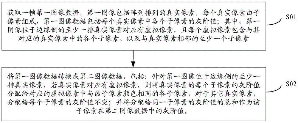
[0044] The embodiment of the present invention provides an image processing method, refer to figure 2 As shown, the method includes:

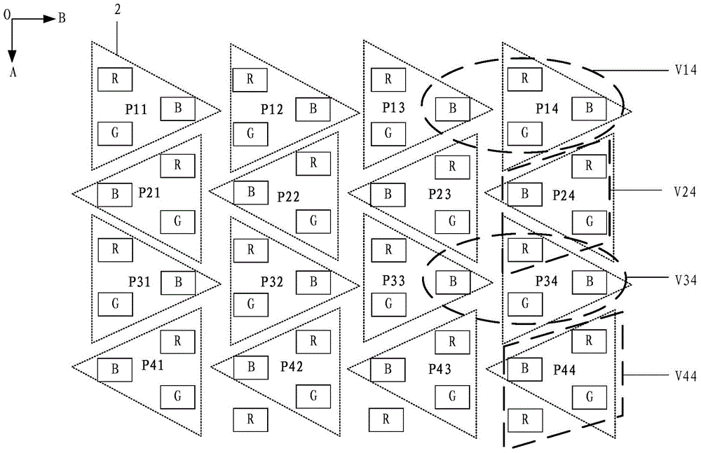
[0045] S01. Obtain a frame of first image data, refer to image 3 As shown, the first image includes real pixels 2 arranged in an array, and each real pixel 2 is composed of sub-pixels, and the first image data includes the gray scale value of each sub-pixel in each real pixel; wherein, the first image is located on the side of the edge At least one row of real pixels corresponds to virtual pixels, and each virtual pixel includes each sub-pixel in the corresponding real pixel and at least one sub-pixel adjacent to the real pixel.

[0046] The number and types of sub-pixels included in each real pixel are not limited. For example, each real pixel may include three sub-pixels: red sub-pixel, green sub-pixel and blue sub-pixel. Of course, in order to improve display brightness , each real pixel can also include four sub-pixels: red sub-pixel, g...

Embodiment 2

[0075] An embodiment of the present invention provides an image processing device, referring to Figure 5 As shown, the above-mentioned devices include:

[0076] An acquisition unit 4, configured to acquire a frame of first image data, the first image includes real pixels arranged in an array, each real pixel is composed of sub-pixels, and the first image data includes grayscale values ​​of each sub-pixel in each real pixel; Wherein, at least one row of real pixels on the edge side of the first image corresponds to virtual pixels, and each virtual pixel includes each sub-pixel in the corresponding real pixel and at least one sub-pixel adjacent to the real pixel.

[0077] The acquisition unit may be a part of a source driver circuit (SourceDriverIntegratedCircuit), such as an input interface.

[0078] The conversion unit 5 is used to convert the first image data into the second image data, including: for at least one row of real pixels on the edge side of the first image, if t...

Embodiment 3

[0085] An embodiment of the present invention provides a display device, including the image processing device provided in Embodiment 2. Embodiments of the present invention provide a display device, which can be display devices such as liquid crystal displays, electronic paper, OLED (Organic Light-Emitting Diode, organic light-emitting diode) displays, and televisions, digital cameras, mobile phones, etc. that include these display devices. Any product or component with a display function, such as a tablet computer.

[0086] optional, see Figure 7 As shown, the display device also includes a packaging substrate 10; the upper surface of the edge of the packaging substrate 10 is an outwardly protruding arc 101, and the lower surface of the edge includes: a downwardly inclined slope 102, connecting the arc 101 and the slope 102 Package side 103 .

[0087] It should be noted that the display device may also include Figure 7 Shown is the array substrate 30 aligned with the pa...


PUM


Abstract

The invention provides an image processing method, a device thereof, and a display device, and relates to the display technology field. By adopting the image processing method, the problems of the edges of the images such as jags and color cast can be improved. The image processing method is characterized in that a frame of first image data can be acquired, and a row of real pixels on an edge side of a first image is provided with corresponding virtual pixels, and every virtual pixel comprises the sub-pixel of the corresponding real pixel and at least one sub-pixel adjacent to the corresponding real pixel; the first image data can be converted into the second image data, and by aiming at the at least one row of real pixels on the edge side of the first image, the gray-scale value of every sub-pixel of each of the real pixels can be allocated to the sub-pixel of the corresponding virtual pixel, the color of which is the same as that of the sub-pixel of the above mentioned real pixel, and the gray-scale value of every other real pixel allocated to every sub-pixel is remained; and the sum total of the gray-scale values allocated to the same sub-pixel can be used as the gray-scale value of the sub-pixel of the second image data. The image processing method is suitable for the display of the display device.

Description

technical field [0001] The present invention relates to the field of display technology, in particular to an image processing method and its device, and a display device. Background technique [0002] AMOLED (ActiveMatrixOrganicLightEmittingDiode, Active Matrix Organic Light Emitting Diode) display devices occupy an important position in the field of display technology. [0003] refer to figure 1 As shown, the AMOLED display device includes a plurality of pixels 1 arranged in an array, and each pixel 1 includes: red sub-pixels R, green sub-pixels G and blue sub-pixels B arranged in a magenta shape. The sub-pixels in each pixel can display different brightness, and each pixel can display different gray levels after mixing. The above-mentioned display device arranged in a character shape has good mixing effect and uniform display picture, and is widely used in AMOLED display devices. but refer to figure 1 As shown, in a column of sub-pixels 100 located on the outermost sid...

Claims


Application Information

Patent Timeline
IPC IPC(8): G09G3/3225
CPCG09G3/3225G09G2300/0439
Inventor 吴渊杨富成季斌蒋璐霞李建军聂军
Owner BOE TECH GRP CO LTD
Learn More