Pixel Array, Electro Optical Device, Electric Apparatus And Method Of Driving Pixel Array

A pixel array and pixel technology, applied in the field of pixel array, can solve the problems of decreased light utilization rate and increased power consumption

Active Publication Date: 2016-07-20
TIANMA MICRO ELECTRONICS CO LTD
View PDF10 Cites 11 Cited by
  • Summary
  • Abstract
  • Description
  • Claims
  • Application Information

AI Technical Summary

Problems solved by technology

The color filter method has the following disadvantages: Since the color filter absorbs light, light utilization efficiency decreases, resulting in increased power consumption, while the side-by-side selective coating method can easily have a wider color gamut due to its high color purity, and The side-by-side selective coating method is widely used due to the improvement of light utilization efficiency without using color filters
Therefore, the corrugated tile arrangement makes an otherwise smooth curve appear as a step-like jagged, or a defect in which color changes are observed as a line in an image that continuously changes in hue or brightness

Method used


Image

  • Pixel Array, Electro Optical Device, Electric Apparatus And Method Of Driving Pixel Array
  • Pixel Array, Electro Optical Device, Electric Apparatus And Method Of Driving Pixel Array
  • Pixel Array, Electro Optical Device, Electric Apparatus And Method Of Driving Pixel Array

Examples


no. 1 example

[0095] Next, refer to Figure 22 to Figure 29 The pixel array and electro-optical device according to the first embodiment will be described.

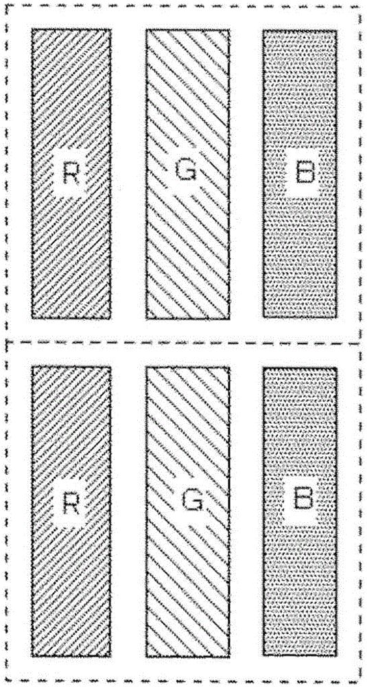
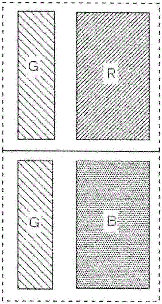
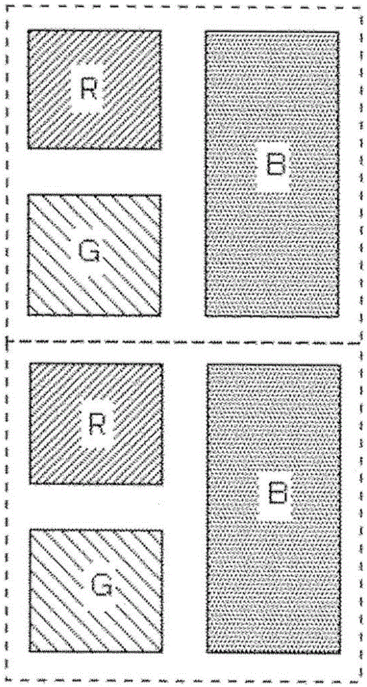
[0096] In the above-mentioned embodiments, the pixel arrangement structure of the electro-optic device (organic EL display device) was particularly described, but this embodiment is concerned with the manufacture of an organic EL display device including a pixel array having the above-mentioned pixel arrangement structure. The method is explained. Figure 22 , Figure 24 , Figure 26 and Figure 28 is has Figure 10 A top view of a pixel of the pixel arrangement shown, while Figure 23 , Figure 25 , Figure 27 and Figure 29 With Figure 22 , Figure 24 , Figure 26 and Figure 28 Correspondingly, for the sake of illustration, a cross-sectional view of a TFT portion, a storage capacitor portion, and a light emitting element shown in one sub-pixel is particularly extracted.

[0097] First, if Figure 22 and Figure 23As ...

no. 2 example

[0108] Next, refer to Figure 30 to Figure 33 An electro-optical device and an electric device according to the second embodiment will be described. In the second embodiment, as an application example of the organic EL display device, various electric equipment including the organic EL display device as a display unit will be described.

[0109] Figure 30 to Figure 33 An example of an electrical device to which an electro-optical device (organic EL display device) is applied is shown. Figure 30 is an example applied to a personal computer, Figure 31 It is an example of application to portable terminal devices such as personal digital assistants (PDAs), electronic notepads, e-books, or tablet terminals. Figure 32 is an example applied to smartphones, and Figure 33 is an example applied to mobile phones. The organic EL display device 400 can be used for display portions of these types of electrical equipment. Applicable to any electrical equipment provided with a disp...

no. 3 example

[0111] Next, refer to Figure 34 to Figure 37 An electro-optical device and electrical equipment according to a third embodiment will be described. In the above-mentioned second embodiment, the case where the organic EL display device as an electro-optical device is applied to an electric device provided with a planar display portion has been described. However, by making the organic EL display device deformable, the organic EL display The device can also be applied to electrical equipment that requires a curved display.

[0112] Figure 34 It is a cross-sectional view showing the structure of a deformable organic EL display device. This structure is different from the above-mentioned first embodiment in that: (1) TFT portion 108 (M1 switch TFT 108a, M2 drive TFT 108b) and storage capacitor portion 109 are formed on a flexible substrate; (2) no sealing glass is arranged on light emitting element 116 Substrate 200.

[0113] First, regarding (1), a peeling film 120 of organi...


PUM


Abstract

The invention relates to a pixel array, electro optical device, an electric apparatus and a method of driving the pixel array. In the pixel array, pixels are two-dimensionally arranged, each of the pixels including a subpixel of the first color having a highest luminosity factor, a subpixel of the second color and a subpixel of the third color having a lowest luminosity factor. A circuit element in each of subpixels of the first color to the third color in each of the pixels is arranged in a row direction. A light emitting region of a subpixel of the first color and a light emitting region of a subpixel of the second color are arranged in the first direction inclined to the row direction. A light emitting region of a subpixel of the third color is arranged in the second direction orthogonal to the first direction, with respect to the light emitting region of the subpixel of the first color and the light emitting region of the subpixel of the second color. The data line extends and is connected to circuit elements in the sub pixels. Data lines connected with the circuit elements in the first color and the light emitting region of the subpixel of the second color, data lines connected with the circuit elements in the second color and the light emitting region of the subpixel of the third color and data lines connected with the circuit elements in the third color and the light emitting region of the subpixel of the first color are arranged repeatedly.

Description

[0001] Cross References to Related Applications [0002] This application claims priority from Patent Application No. 2015-4706 filed in Japan on Jan. 14, 2015, the entire contents of which are incorporated herein by reference. technical field [0003] The present invention relates to a pixel array, an electro-optical device including the pixel array, an electrical device using the electro-optical device as a display device, and a method of driving the pixel array. Background technique [0004] Since the organic electroluminescent (EL) element is a current-driven self-luminous element, it does not require a backlight, and can obtain advantages such as low power consumption, high viewing angle, and high contrast, and is highly anticipated in the development of flat panel displays. . [0005] In an organic EL display device using such an organic EL element, a large number of pixels are constituted by sub-pixels of different colors such as red (R), green (G), and blue (B), wh...

Claims


Application Information

Patent Timeline
Patent Type & Authority Applications(China)
IPC IPC(8): H01L27/32G09G3/3225
CPCG09G3/3225G09G2300/0452H10K59/35H10K59/121H10K59/131G09G3/3233G09G2300/0426H10K59/352H10K59/353G09G3/2003G09G3/2074G09G2320/0666
Inventor 松枝洋二郎高取宪一
Owner TIANMA MICRO ELECTRONICS CO LTD
Why Eureka
Try Eureka