Chip debugging device, debugging method and SOC (System of Chip) chip system

A debugging method and chip technology, applied in the communication field, can solve problems such as inability to debug SOC chip AMBA bus function modules, occupying CPU resources, etc.

Inactive Publication Date: 2016-07-27
ZHEJIANG DAHUA TECH CO LTD
View PDF13 Cites 16 Cited by
  • Summary
  • Abstract
  • Description
  • Claims
  • Application Information

AI Technical Summary

Problems solved by technology

[0007] Embodiments of the present invention provide a chip debugging device, a debugging method, and an SOC chip system, which are used to solve the problems in the prior art that chip debugging takes up CPU resources and cannot debug the functional modules of the AMBA bus inside the SOC chip.

Method used


Image

  • Chip debugging device, debugging method and SOC (System of Chip) chip system
  • Chip debugging device, debugging method and SOC (System of Chip) chip system
  • Chip debugging device, debugging method and SOC (System of Chip) chip system

Examples


Embodiment Construction

[0041] The specific implementation manners of the chip debugging device, the debugging method and the SOC chip system provided by the embodiments of the present invention will be described in detail below with reference to the accompanying drawings.

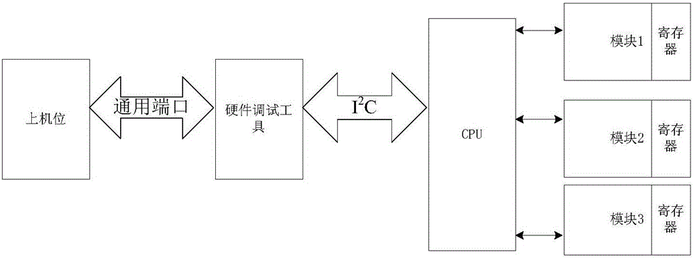
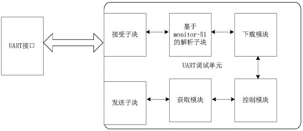
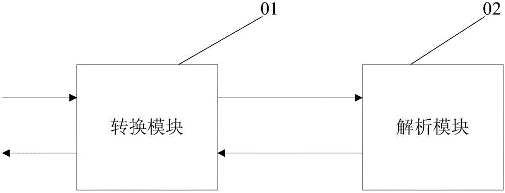
[0042] An embodiment of the present invention provides a chip debugging device for debugging an SOC chip, such as image 3 As shown, the chip debugging device may include: a conversion module 01 and an analysis module 02; wherein, the conversion module 01 is used to convert the external debugging command data received by the SOC chip to the analysis module 02 after serial-to-parallel conversion, and the analysis module 02 The returned data is output after parallel-to-serial conversion; the analysis module 02 is used to analyze the debugging command data converted by the conversion module 01 into an AMBA bus command, and obtain the execution result data of the SOC chip executing the AMBA bus command and return it to the conversion ...


PUM


Abstract

The invention discloses a chip debugging device, a debugging method and an SOC (System of Chip) chip system. The chip debugging device is characterized in that a conversion module carries out serial-parallel conversion on input debugging command data; an analysis module analyzes the debugging command data after serial-parallel conversion into an AMBA (Advanced Microcontroller Bus Architecture) bus command and obtains executive result data obtained by a chip through executing the AMBA bus command, so that a function module in the chip is accessed according to the AMBA bus command, read and write operations are carried out on the function module in the chip and an operation result is returned to the conversion module; and the conversion module outputs the operation result after serial-parallel conversion to complete debugging of the chip. In comparison with the prior art, a chip debugging process of the chip debugging device provided in the embodiments of the invention does not need participation of a CPU (Central Processing Unit), CPU resources are not occupied, and the chip is debugged based on the AMBA bus command, so that the function module in the SOC chip can be debugged, and thus the integrity of chip debugging is improved.

Description

technical field [0001] The invention relates to the field of communication technology, in particular to a chip debugging device, a debugging method and an SOC chip system. Background technique [0002] The SOC (System of Chip) chip contains a CPU (Central Processing Unit), which connects at least two functional modules through a parallel bus. In the development process of the SOC chip, in order to achieve different functions, different functional modules need to be integrated. Inside the SOC chip After the architecture of the SOC chip is built, it is necessary to debug the functional modules inside the SOC chip. [0003] Existing chip debugging scheme: for example scheme 1 (patent application number: CN201010593731.3), such as figure 1 As shown, the chip debugging equipment includes an upper machine position and a hardware debugging tool; the upper machine position is connected with the hardware debugging tool through a general-purpose port, and the hardware debugging tool ...

Claims


Application Information

Patent Timeline
Patent Type & Authority Applications(China)
IPC IPC(8): G06F11/22
CPCG06F11/221G06F11/2273
Inventor 丁明耀
Owner ZHEJIANG DAHUA TECH CO LTD
Why Eureka
Try Eureka