Electrostatic Discharge Protection Structure

An electrostatic discharge protection, conductive type technology, applied in the field of electrostatic discharge protection structures, can solve problems such as uneven conduction of components, and achieve the effect of improving soundness

Active Publication Date: 2019-07-19
UNITED MICROELECTRONICS CORP
View PDF8 Cites 0 Cited by
  • Summary
  • Abstract
  • Description
  • Claims
  • Application Information

AI Technical Summary

Problems solved by technology

Although the finger-shaped protection element can save the die area, this layout method often causes the problem of non-uniform turn-on of the element

Method used


Image

  • Electrostatic Discharge Protection Structure
  • Electrostatic Discharge Protection Structure
  • Electrostatic Discharge Protection Structure

Examples


Embodiment Construction

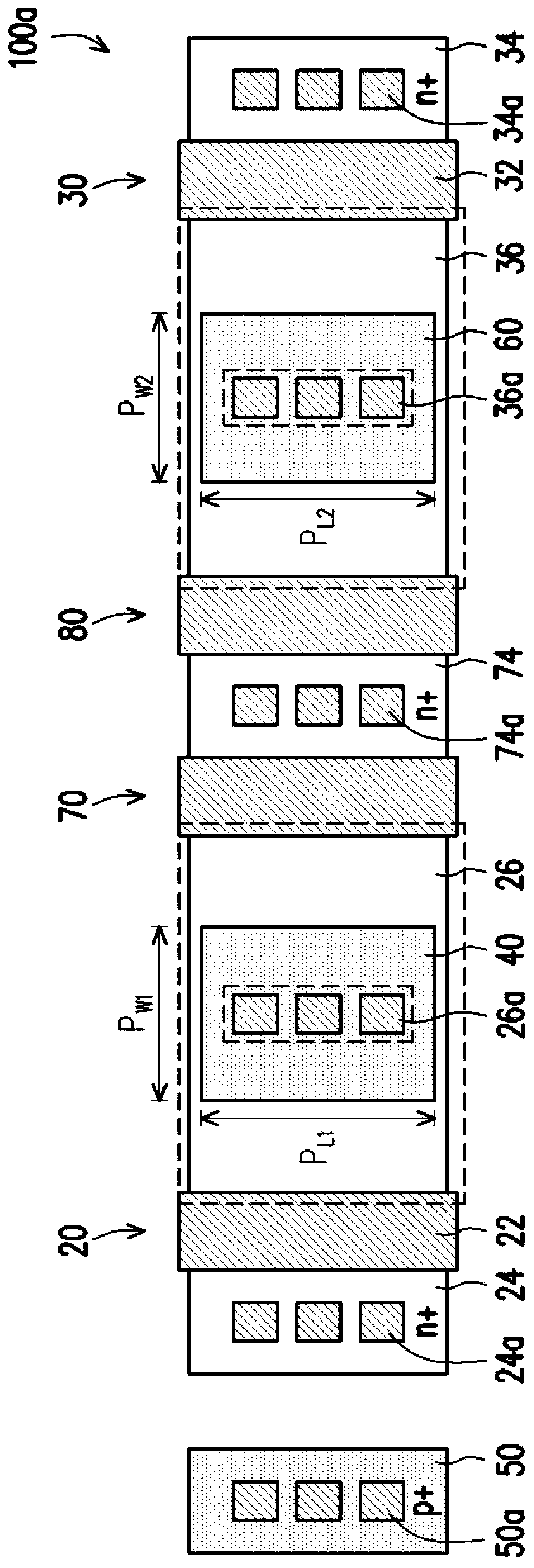
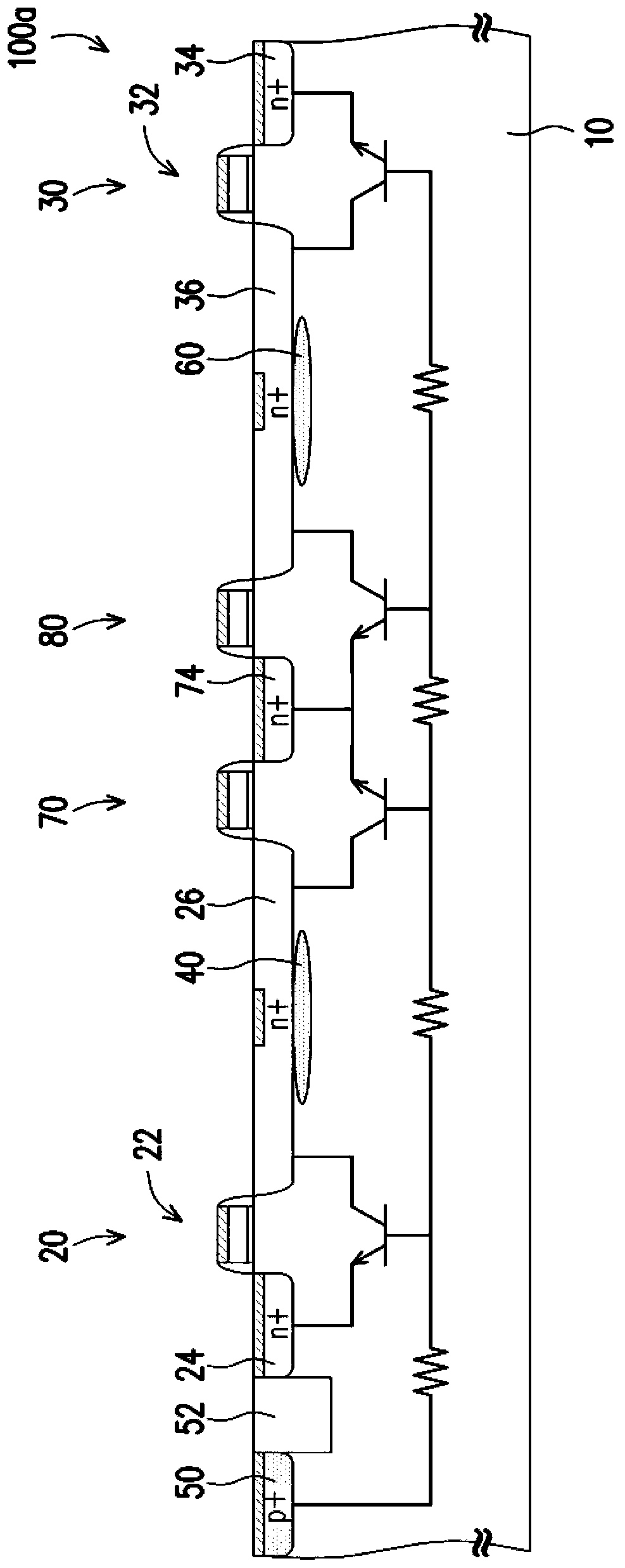
[0052] An electrostatic discharge protection structure according to an embodiment of the present invention includes a plurality of metal oxide semiconductor elements. Under the drain region of each metal oxide semiconductor device, a doped region having a conductivity type different from that of the drain region is provided to improve the soundness of the electrostatic discharge protection structure. Furthermore, the area / doping concentration of the doped region below the drain region close to the pickup region is greater than the area / doping concentration of the doped region below the drain region far away from the pickup region, so that each parasitic BJT The breakdown voltage of each is roughly the same, which in turn makes the turn-on time of each parasitic BJT almost the same.

[0053] figure 1 It is a partial plan view of the electrostatic discharge protection structure of the embodiment of the present invention. figure 2 is a partial cross-sectional schematic diagram...


PUM


Abstract

The invention discloses an electrostatic discharge protection structure. The protection structure comprises a substrate, a contact region, a first metal oxide semiconductor element, a second metal oxide semiconductor element, a first doping region and a second doping region, wherein the contact region is located in the substrate, the first metal oxide semiconductor element comprises a first drain region with a first conducting type and is located in the substrate, the second metal oxide semiconductor element comprises a second drain region with the first conducting type and is located in the substrate; the first drain region is closer to the contact region in comparison with the second drain region; the first doping region and the second doping region are respectively provided with a second conducting type, and respectively located below the corresponding first drain region and the corresponding second drain region; the area and / or doping concentration of the first doping region is greater than the area and / or doping concentration of the second doping area. Through the change of the area / doping concentration of the doping regions, the difference caused by different distances between the doping regions and the contact region can be modified, breakdown voltages of parasitic bipolar transistors (BJT) in different region can be approximately same, so that the breakover time of each BJT is nearly consistent.

Description

technical field [0001] The invention relates to a semiconductor element, and in particular to an electrostatic discharge protection structure. Background technique [0002] Electrostatic discharge (ESD) is a phenomenon in which charges are rapidly moved (discharged) in a short period of time through a discharge path after accumulating on a non-conductor or an ungrounded conductor. Electrostatic discharge can damage circuits made up of components of integrated circuits. For example, a human body, a machine for packaging integrated circuits, or an instrument for testing integrated circuits are common charged objects. When the aforementioned charged objects come into contact with the chip, it is possible to discharge the chip. The instantaneous power of electrostatic discharge can cause damage or failure of the integrated circuits in the chip. [0003] Generally, the electrostatic discharge tolerance of commercial integrated circuits must pass the human body model (HumanBody ...

Claims


Application Information

Patent Timeline
Patent Type & Authority Patents(China)
IPC IPC(8): H01L27/02H01L29/78
Inventor 温詠儒王畅资唐天浩
Owner UNITED MICROELECTRONICS CORP
Why Eureka
Try Eureka