Spurious emission interference suppressing method, spurious emission interference suppressing device and electronic device

A technology of stray interference and suppression devices, which is applied in the direction of line fault/interference reduction, electrical components, transmission systems, etc., which can solve problems such as failure of products to go on the market, impact on system work, and unsatisfactory in-band spectrum templates, so as to improve user experience , improve the quality, and suppress the effect of stray interference components

Active Publication Date: 2016-07-27
GUANGDONG OPPO MOBILE TELECOMM CORP LTD
View PDF5 Cites 19 Cited by
  • Summary
  • Abstract
  • Description
  • Claims
  • Application Information

AI Technical Summary

Problems solved by technology

In-band spurious and interference signals can already affect the normal operation of the system, and cannot be suppressed by filters. Stronger spurious or interference signals may also cause the in-band spectrum template to fail to meet the requirements of the National Radio Commission, resulting in The product cannot be listed
In addition, although out-of-band spurs and interference will not directly affect the normal operation of the system, once intermodulation occurs with other signals, the in-band component of the system may be generated, thereby affecting the system operation

Method used


Image

  • Spurious emission interference suppressing method, spurious emission interference suppressing device and electronic device
  • Spurious emission interference suppressing method, spurious emission interference suppressing device and electronic device
  • Spurious emission interference suppressing method, spurious emission interference suppressing device and electronic device

Examples


Embodiment Construction

[0040] Embodiments of the present invention are described in detail below, and examples of the embodiments are shown in the drawings, wherein the same or similar reference numerals denote the same or similar elements or elements having the same or similar functions throughout. The embodiments described below by referring to the drawings are exemplary, are only for explaining the embodiments of the present invention, and should not be construed as limiting the embodiments of the present invention.

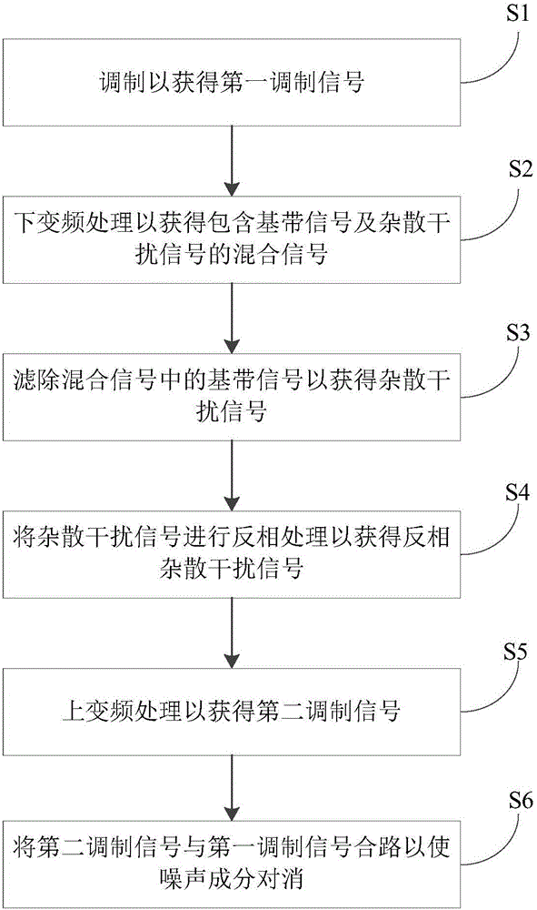
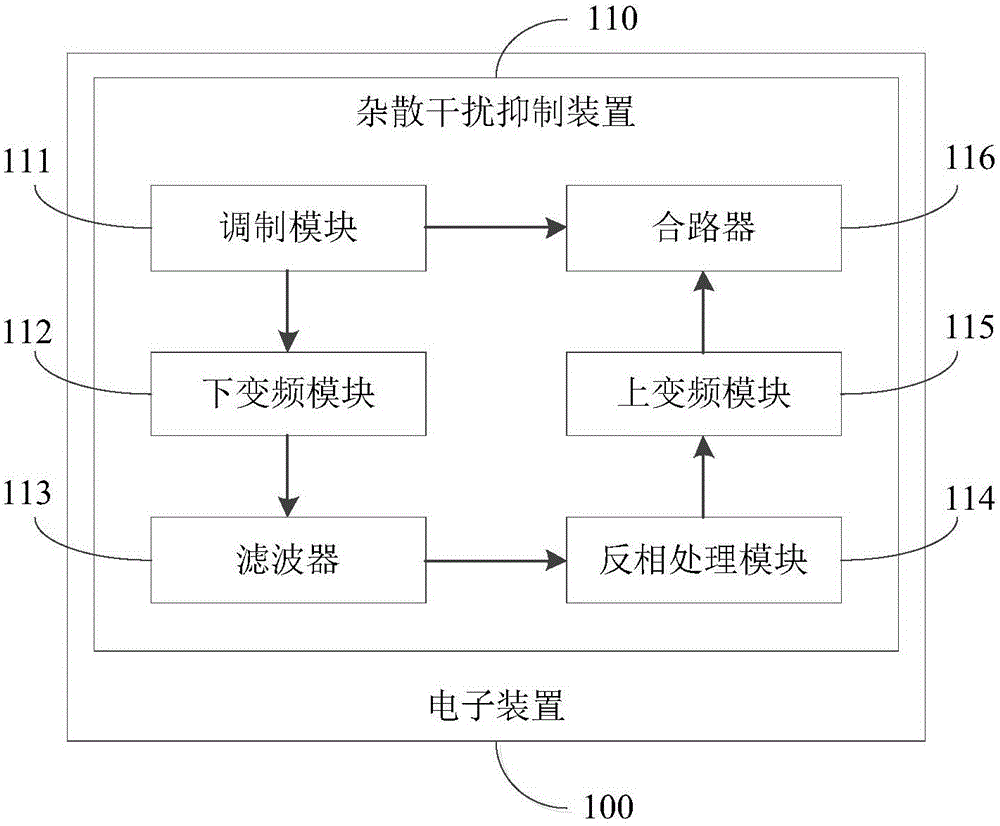
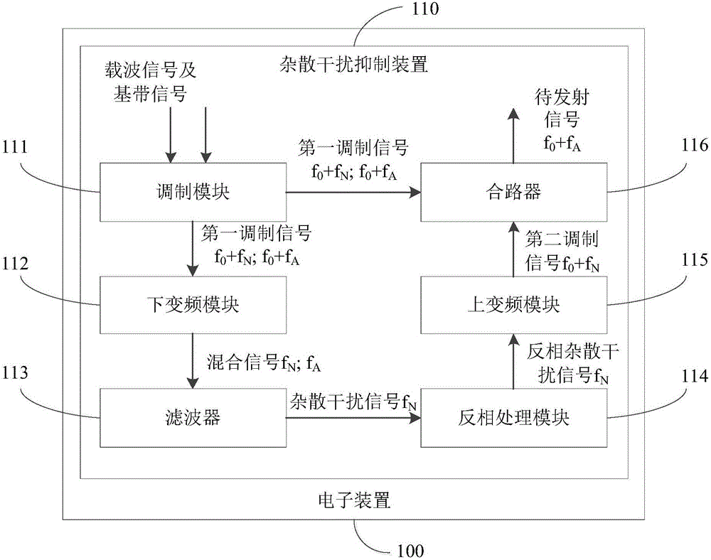
[0041] see Figure 1-3 , the spurious interference suppression method of the embodiment of the present invention can be used to suppress the spurious interference signal of the electronic device 100, and the spurious interference suppression method may include the following steps:

[0042] S1, that is, the modulation step, using the carrier signal to modulate the amplitude of the baseband signal to obtain the first modulated signal;

[0043] S2, that is, the down-conversion step, u...


PUM


Abstract

The invention discloses a spurious emission interference suppressing method, which can be used for suppressing a spurious emission interference signal of an electronic device. The method comprises the following steps: first of all, modulating an amplitude of a baseband signal to obtain a first modulation signal; then, carrying out down-conversion processing on the first modulation signal to obtain a mixed signal comprising the baseband signal and the spurious emission interference signal; after that, filtering the baseband signal in the mixed signal to obtain the spurious emission interference signal; then, carrying out phase reversal processing on the spurious emission interference signal to obtain a phase reversal spurious emission interference signal; then, carrying out up-conversion processing on the phase reversal spurious emission interference signal to obtain a second modulation signal; and at last, combining the second modulation signal and the first modulation signal to enable the spurious emission interference signal to offset the phase reversal spurious emission interference signal. By adopting the spurious emission interference suppressing method or the spurious emission interference suppressing device disclosed by the embodiment of the invention, spurious emission interference elements in the modulation signals can be effectively suppressed, thereby improving the quality of the modulation signals. And the invention further discloses the spurious emission interference suppressing device and the electronic device.

Description

technical field [0001] The invention relates to circuit stray interference suppression technology, in particular to a stray interference suppression method, a stray interference suppression device and an electronic device. Background technique [0002] Noise signals such as spurious interference may appear in the radio frequency circuit. Spurious interference can be divided into out-of-band and in-band. Usually, out-of-band spurs are located outside the system frequency band and will not affect the system. However, the National Radio Commission will control spectrum resources, so the out-of-band spurious indicators The requirements of the national non-committee must be met so that it will not affect other systems or equipment. In-band spurious and interference signals can already affect the normal operation of the system, and cannot be suppressed by filters. Stronger spurious or interference signals may also cause the in-band spectrum template to fail to meet the requiremen...

Claims


Application Information

Patent Timeline
Patent Type & Authority Applications(China)
IPC IPC(8): H04B1/034H04B1/04H04B1/7097H04L25/08
CPCH04B1/0346H04B1/0475H04B1/7097H04B2001/0491H04L25/08
Inventor 韩芸
Owner GUANGDONG OPPO MOBILE TELECOMM CORP LTD
Why Eureka
Try Eureka