

A pixel driving circuit and its driving method, array substrate and display device
A pixel driving circuit and benchmark technology, applied in the field of pixel driving circuit and driving method, array substrate and display device, can solve the problem of high complexity of display panel, and achieve the effect of reducing the number, reducing power consumption and optimizing the driving circuit
- Summary
- Abstract
- Description
- Claims
- Application Information
AI Technical Summary
Problems solved by technology
Method used
Image


Examples
Embodiment 1
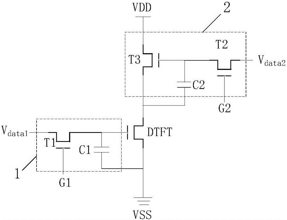
[0062] see figure 2 , The pixel drive circuit includes: a color data writing unit 1, a brightness control unit 2 and a graphene light-emitting device DTFT; the color data writing unit 1 includes a first switching tube T1 and a first storage capacitor C1, wherein the first switching tube T1 The control terminal of the first switch tube T1 receives the first gate control signal G1, and the input terminal of the first switching tube T1 receives the color data signal V data1 (the input end of the first switching tube T1 is connected to the color data line), the output end of the first switching tube T1 is connected to the control terminal of the graphene light-emitting device DTFT; one end of the first storage capacitor C1 is connected to the output end of the first switching tube T1, The other end of the first storage capacitor C1 is connected to the second power supply voltage input terminal VSS; the brightness control unit 2 includes a second switching tube T2, a third switchi...
Embodiment 2
[0072] see image 3 , The pixel driving circuit includes: a color data writing unit 1, a brightness control unit 2, a reference control unit 3 and a graphene light emitting device DTFT; the color data writing unit 1 includes a first switching tube T1 and a first storage capacitor C1, wherein, The control terminal of the first switching tube T1 receives the first grid control signal G1, and the input terminal of the first switching tube T1 receives the color data signal V data1 (the input end of the first switching tube T1 is connected to the color data line), the output end of the first switching tube T1 is connected to the control terminal of the graphene light-emitting device DTFT; one end of the first storage capacitor C1 is connected to the output end of the first switching tube T1, The other end of the first storage capacitor C1 is connected to the second power supply voltage input terminal VSS; the brightness control unit 2 includes a second switching tube T2, a third sw...
PUM
 Abstract
Description
Claims
Application Information