

Semiconductor device, manufacturing method thereof and electronic device
A semiconductor and device technology, applied in the field of semiconductor manufacturing process, can solve problems such as poor contact between the phase change material layer and the bottom electrode, and achieve the effect of avoiding poor contact
Inactive Publication Date: 2016-08-17
SEMICON MFG INT (SHANGHAI) CORP
View PDF5 Cites 1 Cited by
- Summary
- Abstract
- Description
- Claims
- Application Information
AI Technical Summary
Problems solved by technology
However, the top of the bottom electrode formed by the prior art is lower than the opening of the groove used to fill the bottom electrode, that is, this phenomenon occurs after the bottom ele
Method used
View moreImage
Smart ImageViewing Examples

Examples
 PUM
| Property | Measurement | Unit |
|---|---|---|
| Thickness | aaaaa | aaaaa |
| Thickness | aaaaa | aaaaa |
| Thickness | aaaaa | aaaaa |
Abstract
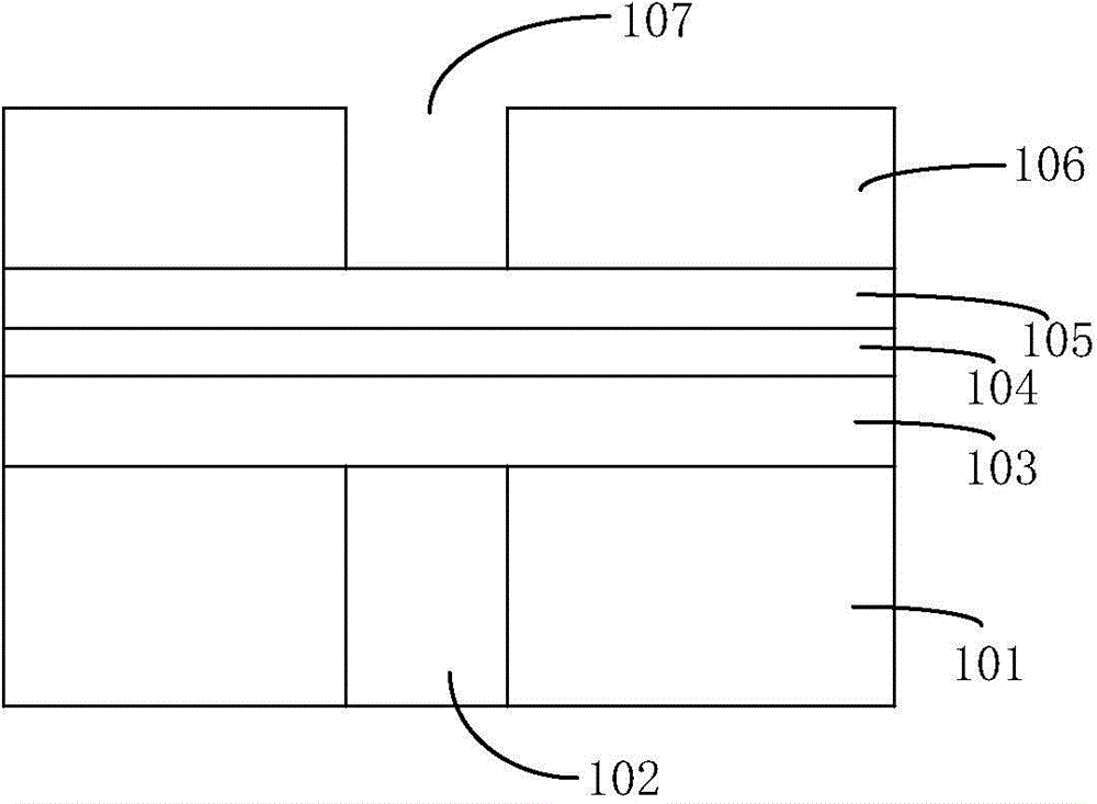
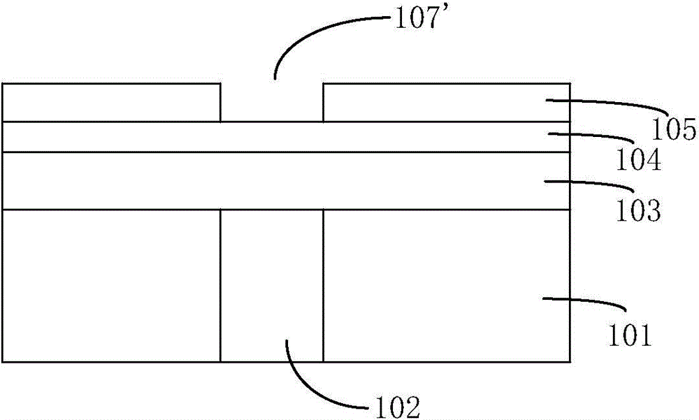
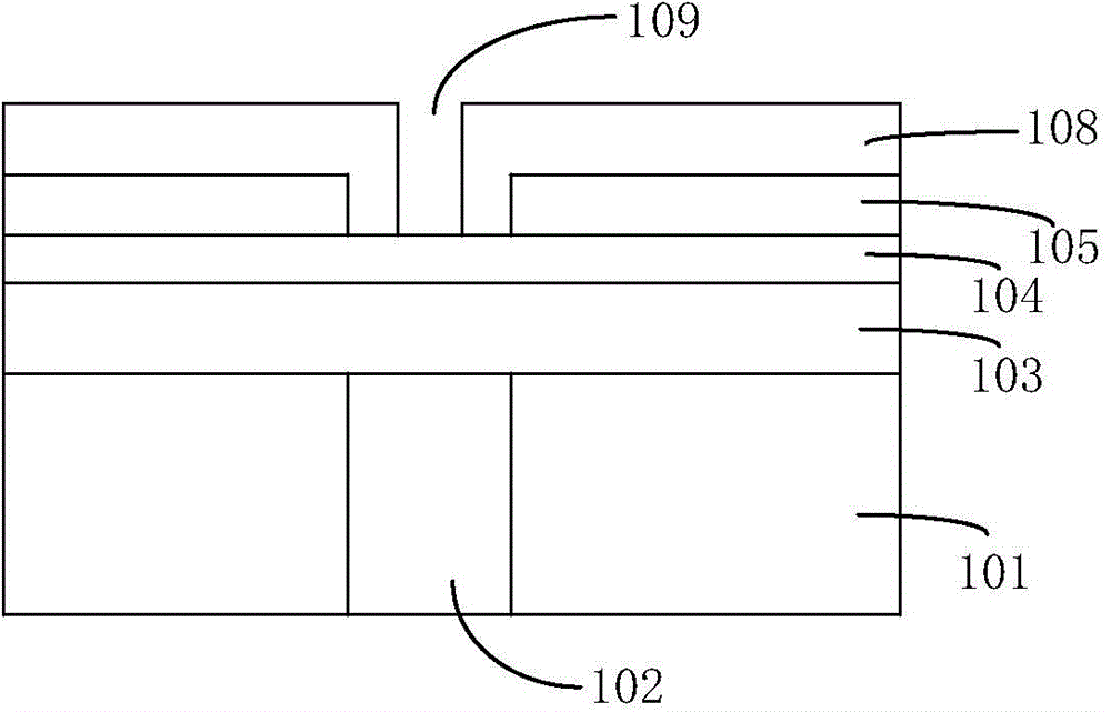
The present invention provides a semiconductor device, a manufacturing method thereof and an electronic device. The method includes the following steps that: a semiconductor substrate is provided, an interlayer dielectric layer is formed on the semiconductor substrate, and a metal electrode is formed in the interlayer dielectric layer; a hard mask stack structure is formed on the interlayer dielectric layer so as to cover the interlayer dielectric layer and the metal electrode, wherein the hard mask stack structure includes a first buffer layer, a grinding stop layer, a second buffer layer, a first hard mask layer and a second hard mask layer which are stacked from bottom to top; a through hole which can be filled with a bottom electrode material layer is formed in the hard mask stack structure; the bottom electrode material layer is deposited until the bottom electrode material layer completely fills the through hole; chemical mechanical grinding is performed until the grinding stop layer is exposed; and back etching is carried out, so that the grinding stop layer can be removed, and the top end of the formed bottom electrode can be higher than the top end of the first buffer layer. With the manufacturing method provided by the present invention adopted, poor contact between a phase changing material layer which is formed in a follow-up step and the bottom electrode can be avoided.
Description
technical field [0001] The invention relates to a semiconductor manufacturing process, in particular to a semiconductor device, a manufacturing method thereof, and an electronic device. Background technique [0002] Phase change memory (PCM) is a type of memory with high read / write speed, which is widely used in integrated circuits. The key step of integrated phase change memory is to form the bottom electrode (Bottom Electrode) for connecting the metal electrode and the phase change material layer, and the bottom electrode contacts the phase change material layer from the bottom of the phase change material (GST) layer. When a certain intensity of current passes through the bottom electrode, the bottom electrode generates Joule heat to change the phase change state of the phase change material layer, thereby controlling the working state of the phase change memory, that is, when the phase change material layer changes from an amorphous state to a crystalline state. The fun...
Claims
Login to View More Application Information
Patent Timeline
 IPC IPC(8): H01L21/768H01L27/24H01L45/00
Inventor周耀辉汪新学
OwnerSEMICON MFG INT (SHANGHAI) CORP