Display device

一种显示装置、氧化物半导体的技术,应用在产品或组合物,机器,工序,半导体装置领域,能够解决难绝缘表面的大面积衬底处理等问题,达到耗电量低、实现小型化、减少图像质量的效果

Active Publication Date: 2016-08-17
SEMICON ENERGY LAB CO LTD
View PDF9 Cites 2 Cited by
  • Summary
  • Abstract
  • Description
  • Claims
  • Application Information

AI Technical Summary

Problems solved by technology

Due to this limitation, it is difficult to process large-area substrates with insulating surfaces in a short time

Method used


Image

  • Display device
  • Display device
  • Display device

Examples


Embodiment approach 1

[0101] In this embodiment mode, a semiconductor device according to one embodiment of the present invention and a method of manufacturing the semiconductor device will be described with reference to the drawings. Here, as an example of a semiconductor device, refer to figure 1 , figure 2 , Figures 3A to 3C , Figure 4A and 4B as well as Figure 5A and 5B A liquid crystal display device and a light emitting device will be described. In the present embodiment, each of the semiconductor devices includes a first transistor and a second transistor, and the first transistor and the second transistor include oxide semiconductor films whose structures are different.

[0102]

[0103] First, a liquid crystal display device will be described.

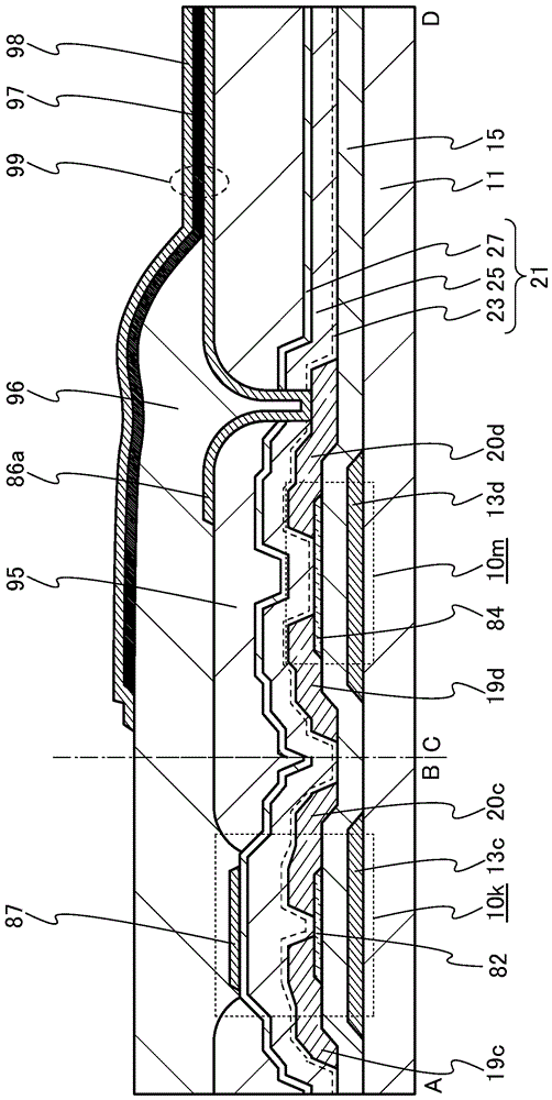
[0104] figure 1 is a cross-sectional view of the liquid crystal display device. Transistors formed in the driver circuit section are shown in section A-B, and transistors formed in the pixel section are shown in section C-D.

[0105...

Deformed example 1

[0228] figure 1 The liquid crystal display device shown and figure 2 The illustrated light-emitting device may include a transistor in which two layers of oxide semiconductor films are stacked. Here, explain figure 1 A modified example of the liquid crystal display device shown. Specifically, as Figure 26 As shown, there are provided: a transistor 10k_1 in which an oxide semiconductor film 81 and an oxide semiconductor film 82 are stacked on a gate insulating film 15; 84 transistors 10m_1.

[0229] In the oxide semiconductor film 81 and the oxide semiconductor film 81a, the ratio of In atoms may be greater than or equal to the ratio of Zn or M (M is Al, Ga, Y, Zr, La, Ce, or Nd) atoms. The oxide semiconductor film 81 and the oxide semiconductor film 81a contain In-M-Zn oxide (M is Al, Ga, Y, Zr, La, Ce, or Nd), and the atomic ratio of the metal elements used is In:M. : Zn=x 3 :y 3 :z 3 In the case of forming the oxide semiconductor film 81 and the oxide semiconducto...

Deformed example 2

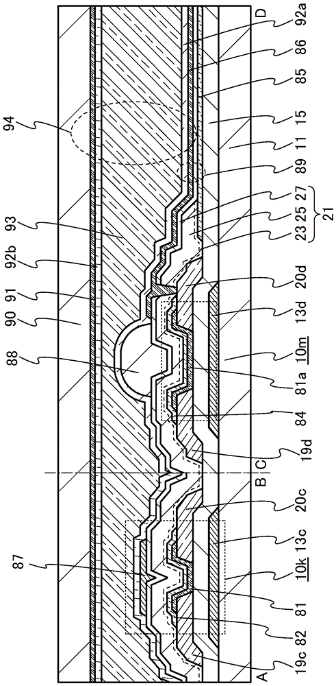
[0232] figure 1 The liquid crystal display device shown and figure 2 The light-emitting device shown may have transistors in which three or more oxide semiconductor films are stacked. Here, explain figure 2 Variations of the light-emitting device shown. Specifically, as Figure 27 As shown in FIG. 83a, the oxide semiconductor film 81a, and the transistor 10m_2 of the oxide semiconductor film 84.

[0233] As the oxide semiconductor film 83 and the oxide semiconductor film 83a, an oxide semiconductor having the atomic ratio given as an example of the atomic ratio of the metal elements in the oxide semiconductor film 82 and the oxide semiconductor film 84 can be suitably used. membrane. In addition, among the stacked oxide semiconductor films, the oxide semiconductor films 81 and 81 a serving as channel regions of transistors have the thickest thickness. The oxide semiconductor films 81 and 81 a have a thickness of 3 nm or more and 200 nm or less, preferably 3 nm or more...


PUM

PropertyMeasurementUnit
lengthaaaaaaaaaa
lengthaaaaaaaaaa
lengthaaaaaaaaaa

Abstract

An object of the present invention is to provide a display device in which plural kinds of circuits are formed over one substrate and plural kinds of transistors corresponding to characteristics of the plural kinds of circuits are provided. The display device includes a pixel portion and a driver circuit that drives the pixel portion over one substrate (11). The pixel portion includes a first transistor (10m) including a first oxide semiconductor film (84). The driver circuit includes a second transistor (10k) including a second oxide semiconductor film (82). The first oxide semiconductor film (84) and the second oxide semiconductor film (82) are formed over one insulating surface. A channel length of the first transistor (10m) is longer than a channel length of the second transistor (10k). The channel length of the first transistor (10m) is greater than or equal to 2.5 micrometer.

Description

technical field [0001] The present invention relates to an object, method or method of manufacture. In addition, the present invention relates to a process (process), machine (machine), product (manufacture) or composition (composition of matter). In particular, the present invention relates to a semiconductor device, a display device, a light emitting device, an electrical storage device, a memory device, a driving method thereof, or a manufacturing method thereof. In particular, the present invention relates to a semiconductor device including a field effect transistor. [0002] In this specification and the like, a semiconductor device generally refers to a device that can function by utilizing semiconductor characteristics. A semiconductor element such as a transistor, a semiconductor circuit, an arithmetic device, and a storage device are all one form of a semiconductor device. Imaging devices, display devices, liquid crystal display devices, light-emitting devices, el...

Claims


Application Information

Patent Timeline
Patent Type & Authority Applications(China)
IPC IPC(8): G09F9/30G02F1/1345G02F1/1368H01L21/316H01L21/318H01L21/363H01L29/786H01L51/50
CPCH01L29/78648H01L29/78696H01L27/1251H01L29/7869H01L27/1225H10K59/1213H10K59/1201H01L27/1248
Inventor 山崎舜平冈崎健一片山雅博
Owner SEMICON ENERGY LAB CO LTD
Why Eureka
Try Eureka