SON (Silicon on Nothing) deformation mechanism study method based on phase field model at high temperature

A silicon-based microstructure and model technology, applied in the micro-nano field, can solve problems such as the limitations of understanding particle diffusion

Active Publication Date: 2016-09-21
嘉兴华吉环保科技有限公司
View PDF4 Cites 8 Cited by
  • Summary
  • Abstract
  • Description
  • Claims
  • Application Information

AI Technical Summary

Problems solved by technology

[0004] In recent years, the industry has devoted itself to using mathematical models to analyze and calculate the diffusion between particles, but th

Method used


Image

  • SON (Silicon on Nothing) deformation mechanism study method based on phase field model at high temperature
  • SON (Silicon on Nothing) deformation mechanism study method based on phase field model at high temperature
  • SON (Silicon on Nothing) deformation mechanism study method based on phase field model at high temperature

Examples


Embodiment Construction

[0049] The preferred embodiments of the present invention will be described in detail below in conjunction with the accompanying drawings.

[0050] The drawings involved in this embodiment are all simplified schematic diagrams, and only illustrate the basic structure of the present invention in a schematic manner, therefore, only the structures related to the present invention are shown.

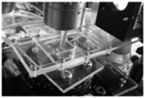
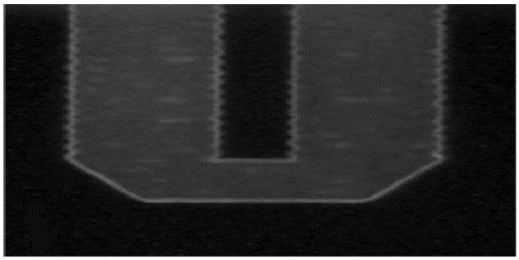
[0051] build as figure 1 As shown in the experimental bench, the silicon-based microstructure material used is a polished 6-in (100) n-type silicon wafer; the raw material is put into an environment of 88° C. to make it soft for 90 seconds; the processed The samples were produced using ion etching machine as figure 2 The U-shaped cylindrical hole shown;

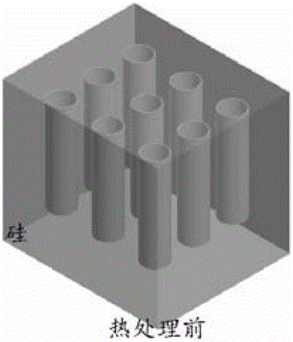
[0052] like image 3 As shown, the above-mentioned U-shaped cylindrical hole sample was placed in an environment of 1150 ° C for 3 minutes;

[0053] like Figure 4As shown, the schematic diagram of the morphology change of the silicon...


PUM


Abstract

The invention discloses an SON (Silicon on Nothing) deformation mechanism study method based on a phase field model at a high temperature. The method comprises the following steps of 1, putting a sample, i.e., an SON material at a certain temperature so that the sample becomes soft, and then making the sample into a U-shaped cylindrical hole shape; 2, putting the SON material into a high-temperature environment to be processed for several minutes for obtaining the SON form change state in different time periods; and 3, building a system model of the SON at the high temperature. According to the method, the SON deformation mechanism at the high temperature is studied by the method of integrating the experiment study and the simulation model for the first time. The SON forming process is controlled by using the high-temperature atomic diffusion motion; through the simulation model, the SON forming change can be more directly observed; and thus, a novel idea for processing the SON is provided.

Description

technical field [0001] The invention belongs to the field of micro-nano technology, and in particular relates to a research method for the deformation mechanism of silicon-based microstructures based on a phase field model at high temperature. Background technique [0002] Silicon material is one of the main materials for MEMS (Micro-Electro-Mechanical Systems) manufacturing. A three-dimensional structure with a size of micron is produced on a silicon chip to realize the perception and control of external information, which can constitute a multifunctional micro system. In recent years, various disciplines have been persistently trying various new science and technology, trying to use various methods to design and manufacture silicon-based microstructure Silicon on nothing (SON) for various mechanical devices, such as: sensors, semiconductor transistors . However, so far, how to control the preparation of the SON structure, so that it can be applied to resonators with diffe...

Claims


Application Information

Patent Timeline
IPC IPC(8): G06F17/50
CPCG06F30/367
Inventor 张俐楠郑伟吴立群
Owner 嘉兴华吉环保科技有限公司
Why Eureka
Try Eureka