Display panel and manufacturing method thereof

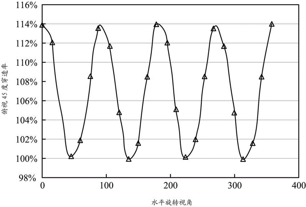
A display panel and manufacturing method technology, applied in the direction of instruments, nonlinear optics, optics, etc., can solve the problems of increased transmittance of display panels, obvious changes in brightness and darkness, poor visual experience, etc., and achieve horizontal rotation penetration Improvement of change in transmittance and low loss of aperture ratio

Inactive Publication Date: 2016-10-05
INNOLUX CORP
View PDF7 Cites 2 Cited by
  • Summary
  • Abstract
  • Description
  • Claims
  • Application Information

AI Technical Summary

Problems solved by technology

[0003] However, while the area of ​​the dark pattern is reduced as much as possible, it will increase the transmittance variation of the display panel at different angles in the horizontal rotation viewing angle.
refer to figure 1 , when the existing display panel is rotated horizontally, it will be found that the transmittance of the horizontally rotated viewing angle of the display panel has a change of about 14% (114% to 100%) when viewed from a 45-degree viewing angle. Too obvious, resulting in poor visual experience

Method used


Image

  • Display panel and manufacturing method thereof
  • Display panel and manufacturing method thereof
  • Display panel and manufacturing method thereof

Examples


Embodiment Construction

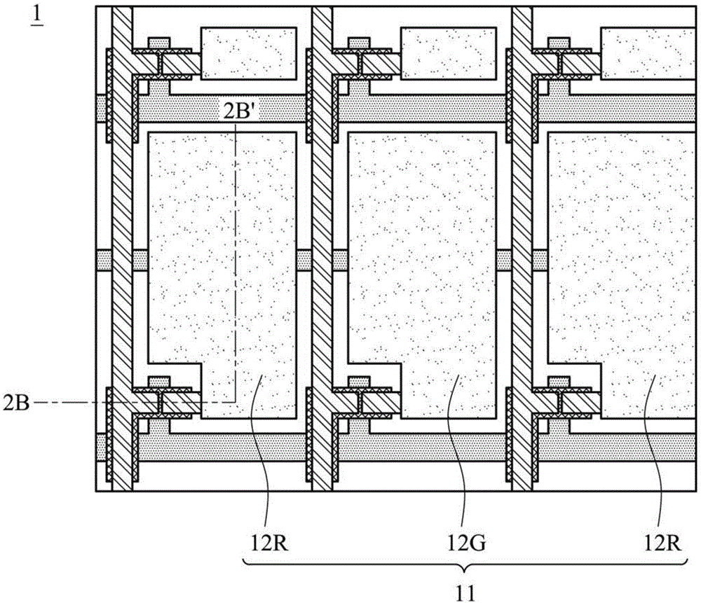
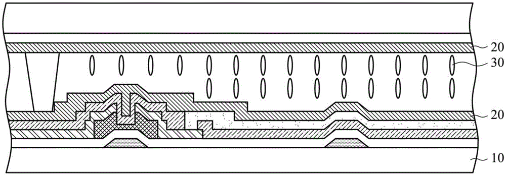
[0055] refer to Figure 2A , Figure 2B , Figure 2A A partially enlarged view showing the thin film transistor substrate 10 of the display panel 1 according to the embodiment of the present invention, Figure 2B for Figure 2A 2B-2B' in the sectional view, the display panel 1 includes a thin film transistor substrate 10 , a photo-alignment layer 20 and a liquid crystal layer 30 . collocation reference Figure 2A , Figure 2B , the thin film transistor substrate 10 has a plurality of pixel units 11, wherein each pixel unit 11 has a plurality of sub-pixels 12, in one embodiment, each pixel unit 11 has a red sub-pixel 12 (R), a green sub-pixel 12 (G) and blue sub-pixel 12 (B). The photo-alignment layer 20 is formed on the TFT substrate 10 and located on the pixel units 11 , and has at least two alignments in different directions corresponding to each of the sub-pixels 12 . The liquid crystal layer 30 is disposed on the alignment layer 20 and has a plurality of liquid crys...


PUM

PropertyMeasurementUnit
angleaaaaaaaaaa

Abstract

A display panel and a manufacture method are provided. The display panel includes a TFT substrate (100) and a photo-alignment layer. The TFT substrate includes a plurality of pixel units, wherein each pixel unit includes a plurality of sub-pixels. The photo-alignment layer is located on the pixel units, and has at least two different aligning directions corresponding to each sub-pixel. When light passes through each sub-pixel, the display panel shows a dark line pattern. The dark line pattern includes a major line and a minor line. The major line is located on the boundary between the two different aligning directions in the photo-alignment layer, and extends along a first direction, wherein the major line has a major line width. The minor line is connected to the major line, and extends along a second direction, wherein the minor line has a minor line width, and the major line width is greater than the minor line width.

Description

technical field [0001] The invention relates to a display panel, in particular to a display panel with a photo-alignment layer. Background technique [0002] Existing display panels include thin film transistor substrates, photo-alignment layers, liquid crystal layers and other elements. The existing photo-alignment layer manufacturing process first forms an alignment layer on the thin-film transistor substrate, and then uses alignment masks aligned in different directions to cover different parts of the thin-film transistor substrate with the alignment layer, and then passes through the exposure step. Photo-alignment layers with different orientations are formed on the TFT substrate. In the prior art, when a light passes through each sub-pixel of the TFT substrate having photo-alignment layers aligned in different directions, the display panel will display a dark pattern. In order to increase the aperture ratio of the display panel, the existing concept tends to reduce th...

Claims


Application Information

Patent Timeline
Patent Type & Authority Applications(China)
IPC IPC(8): G02F1/1333G02F1/1337
CPCG02F1/133753G02F1/133788G02F1/1393G02F1/133776G02F1/133757G02F1/1337G02F1/1368
Inventor 崔博钦黄鹏丞朱夏青
Owner INNOLUX CORP
Why Eureka
Try Eureka