Shifting register and drive method thereof, grid drive circuit and display device

A shift register, potential technology, applied in static memory, digital memory information, instruments, etc., can solve problems such as unfavorable narrow borders and large space occupied by gate drive circuits

Inactive Publication Date: 2016-10-12
BOE TECH GRP CO LTD +1
View PDF6 Cites 90 Cited by
  • Summary
  • Abstract
  • Description
  • Claims
  • Application Information

AI Technical Summary

Problems solved by technology

[0004] However, each stage of the shift register in the existing gate drive circuit can only be used to drive one row of gate lines, so the entire gate drive circuit occupies a large space, which is not conducive to the realization of narrow borders

Method used


Image

  • Shifting register and drive method thereof, grid drive circuit and display device
  • Shifting register and drive method thereof, grid drive circuit and display device
  • Shifting register and drive method thereof, grid drive circuit and display device

Examples


Embodiment 1

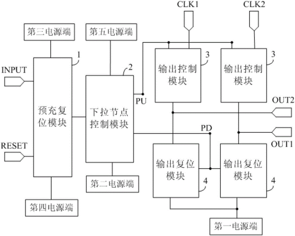
[0062] figure 1 A schematic structural diagram of a shift register provided in Embodiment 1 of the present invention, as shown in figure 1 As shown, the shift register includes: a pre-charge reset module 1, a pull-down node control module 2, several output control modules 3 and several output reset modules 4, the output reset modules 4 correspond to the output control modules 3 one-to-one, and the pre-charge The reset module 1, the pull-down node control module 2 and each output control module 3 are connected to the pull-up node PU, and the output control module 3 and each output reset module 4 are connected to the pull-down node PD.

[0063] Wherein, the precharge reset module 1 is used for precharging or resetting the pull-up node PU under the control of the precharge signal input from the precharge signal input terminal INPUT and the reset signal input from the reset signal input terminal RESET.

[0064] The pull-down node control module 2 is used to control the potential ...

Embodiment 2

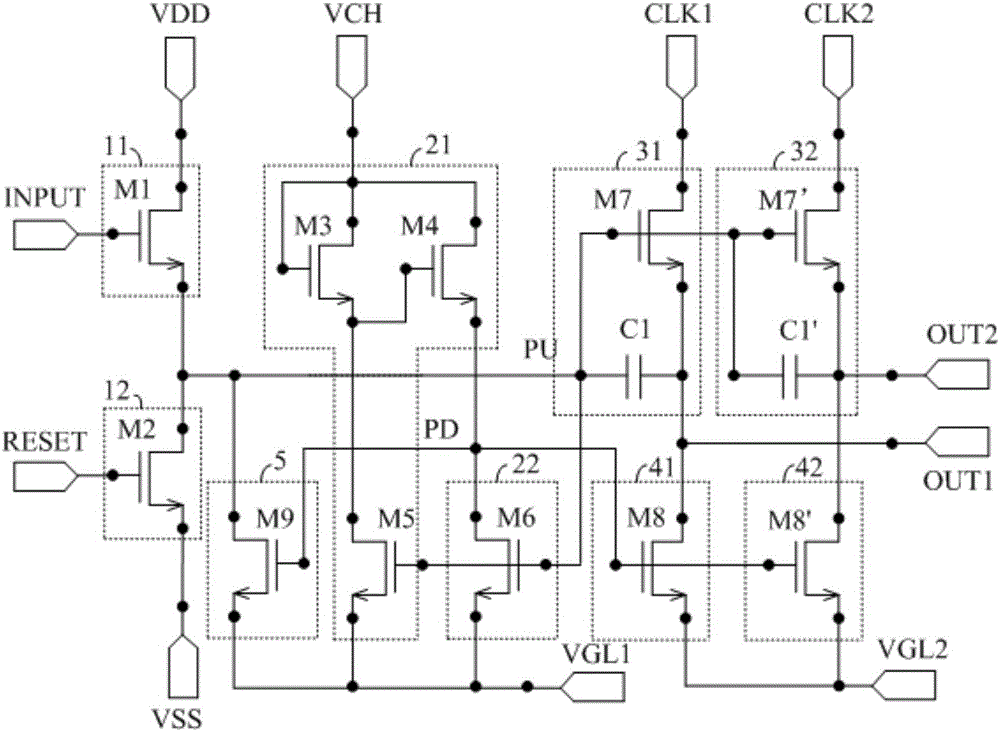
[0074] figure 2 The circuit schematic diagram of the shift register provided for the second embodiment of the present invention, such as figure 2 as shown, figure 2 The circuit diagram shown is figure 1 The embodiment of the shown structure diagram, in this embodiment, will be exemplarily described by taking two output control modules 31 / 32 and two output reset modules 41 / 42 as an example.

[0075] In this embodiment, optionally, each output control module 31, 32 includes a seventh transistor M7 / M7' and a capacitor C1 / C1'; the control electrode of the seventh transistor M7 / M7' and the pull-up node PU connection, the first pole is connected to the corresponding clock control signal line CLK1 / CLK2, the second pole is connected to the corresponding signal output terminal OUT1 / OUT2; the first terminal of the capacitor C1 / C1' is connected to the pull-up node PU, and the second terminal It is connected with the second pole of the seventh transistor M7 / M7'.

[0076] Optionally...

Embodiment 3

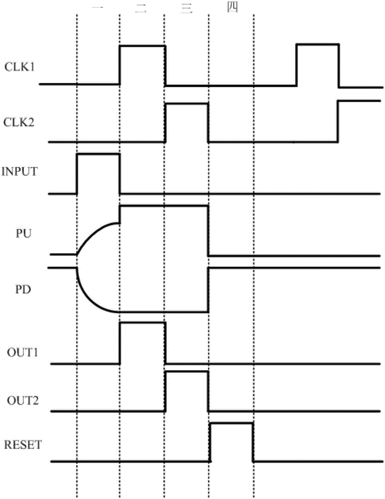
[0106] Figure 4 The flow chart of the driving method of the shift register provided by Embodiment 3 of the present invention, such as Figure 4 As shown, wherein, the shift register can adopt the shift register in the above-mentioned embodiment 1 or embodiment 2, and the driving method includes:

[0107] Step 101, the precharge reset module precharges the pull-up node under the control of the precharge signal input by the precharge signal input terminal, and the pull-down node control module pulls down the potential of the pull-down node under the control of the potential of the pull-up node ;

[0108] Step 102, each output control module sends the clock control signal in the corresponding clock control signal line to the corresponding signal output terminal under the control of the potential of the pull-up node, so that the signal output terminal outputs the scanning signal;

[0109] Step 103, the precharge reset module resets the pull-up node under the control of the rese...


PUM


Abstract

The invention discloses a shifting register and a drive method thereof, a grid drive circuit and a display device. The shifting register comprises a precharge reset module, a downward-pull node control module, a plurality of output control modules and a plurality of output reset modules. The output reset modules correspond to the output control modules one to one. The output control modules are used for transmitting clock control signals in corresponding clock control signal lines to corresponding signal output ends under control of potential of upward-pull nodes. The output reset modules are used for resetting the signal output ends connected with the corresponding output control modules under control of potential of downward-pull nodes. The shifting register is provided with the signal output ends, the output control modules for controlling the signal output ends to output the signals and the output reset modules, the shifting register can be used for driving a plurality of grid lines, and therefore the shifting register can achieve design of an ultra-narrow frame when applied to a display panel.

Description

technical field [0001] The invention relates to the field of display technology, in particular to a shift register, a driving method thereof, a gate driving circuit and a display device. Background technique [0002] The basic principle of TFT-LCD (Thin Film Transistor-Liquid Crystal Display, thin film transistor liquid crystal display device) to realize a frame display is to input a square wave of a certain width to each row of pixels sequentially from top to bottom through the gate (Gate) drive. Strobe, and then drive the signal required for each row of pixels through the source (Source) and output from top to bottom in turn. At present, the display device with such a structure is usually made of gate drive circuit and source drive circuit on the glass panel by COF (Chip On Film, chip-on-film) or COG (Chip On Glass, chip directly fixed on the glass) process. However, when the resolution is high, the output of the gate drive circuit and the source drive circuit will increa...

Claims


Application Information

Patent Timeline
Patent Type & Authority Applications(China)
IPC IPC(8): G09G3/36G11C19/28
CPCG09G3/3674G11C19/28
Inventor 李金钰马磊
Owner BOE TECH GRP CO LTD
Why Eureka
Try Eureka