Integrated circuit device, display panel and display device

A technology of integrated circuits and display substrates, applied in the field of fingerprint identification, can solve the problems of increased production cost of protective layer, influence of screen ratio, increase of production process cost, etc., to reduce production cost, increase screen ratio, and signal penetration strong effect

Active Publication Date: 2016-10-26
BOE TECH GRP CO LTD
View PDF6 Cites 15 Cited by
  • Summary
  • Abstract
  • Description
  • Claims
  • Application Information

AI Technical Summary

Problems solved by technology

[0005] The defect of the above-mentioned prior art is that the capacitive fingerprint recognition module is arranged at the opening position of the front panel, which will not only increase the manufacturing process cost, but also affect the screen ratio; will increase production cost

Method used


Image

  • Integrated circuit device, display panel and display device
  • Integrated circuit device, display panel and display device
  • Integrated circuit device, display panel and display device

Examples


Embodiment Construction

[0029] In order to solve the technical problems of low screen-to-body ratio and high manufacturing cost of current display devices with fingerprint recognition functions, embodiments of the present invention provide an integrated circuit (integrated circuit, hereinafter referred to as IC) device, a display panel, and a display device. In order to make the purpose, technical solution and advantages of the present invention clearer, the following examples are given to further describe the present invention in detail.

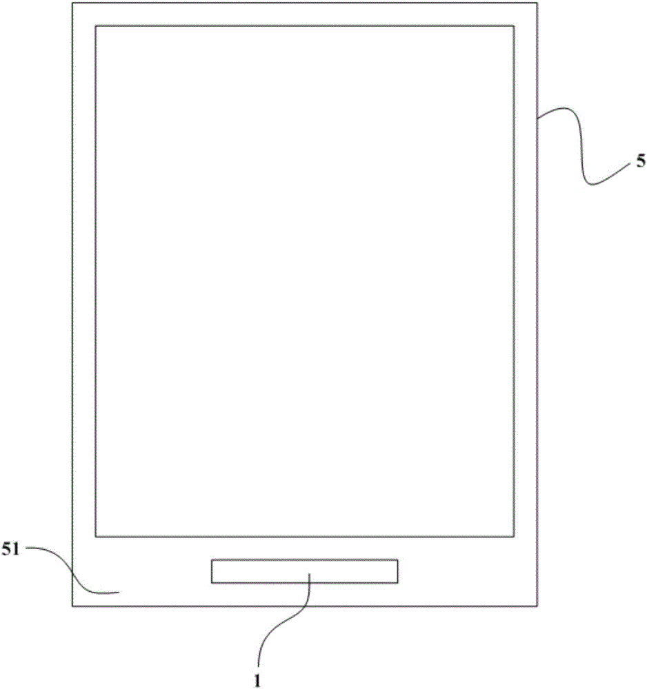
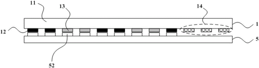
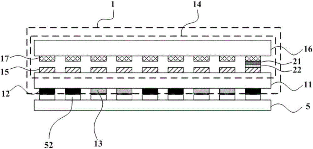
[0030] Such as figure 1 and figure 2 As shown, the IC device 1 provided by an embodiment of the present invention includes a first substrate 11 and a plurality of touch signal terminals 12 and a plurality of display signal terminals 13 arranged on the first substrate 11. The plurality of touch signal terminals Terminal 12 and the plurality of display signal terminals 13 are used for corresponding binding connection with a plurality of connection signal terminals...


PUM


Abstract

The present invention discloses an integrated circuit device, a display panel and a display device. The integrated circuit device comprises a first substrate and a plurality of touch signals and a plurality of display signal terminals arranged on the first substrate, the touch signals and the display signal terminals are configured to perform corresponding binding connection with a plurality of connection signals arranged by a non-display area of the display substrate, and the integrated circuit device also comprises an supersonic wave fingerprint identification device arranged on the first substrate. The integrated circuit device is applied to the display device which has a fingerprint identification function and has front panel which does not need to reserve an opening like a fingerprint identification module in the prior art, and therefore the screen rate of the display device can be improved; and moreover, because the penetrability of signals of the supersonic wave fingerprint identification device is high, and therefore, a protective layer with harshly required thickness is not needed, and the manufacturing cost of the display device is greatly reduced.

Description

technical field [0001] The invention relates to the technical field of fingerprint identification, in particular to an integrated circuit device, a display panel and a display device. Background technique [0002] With the in-depth study of human physiological characteristics in user identification, fingerprint recognition has been widely used in various electronic devices such as smartphones and tablets to simplify the user's tasks in various scenarios such as screen unlocking and transaction payment. operation and contribute to increased safety. [0003] At present, the fingerprint identification technology commonly used in various mobile terminals is capacitive fingerprint identification technology, which manufactures multiple fingerprint electrodes on a silicon substrate, and each fingerprint electrode is used as a plate of the capacitor, and the finger is used as the other electrode of the capacitor. According to the capacitance difference between the ridges and valley...

Claims


Application Information

Patent Timeline
Patent Type & Authority Applications(China)
IPC IPC(8): G06K9/00H01L27/12H01L21/77
CPCH01L27/12H01L21/77G06V40/1306
Inventor 刘英明董学薛海林王海生陈小川丁小梁杨盛际许睿李昌峰刘伟王鹏鹏
Owner BOE TECH GRP CO LTD
Why Eureka
Try Eureka