
Eureka
For R&D, Eureka makes reading and utilizing patents & technical documents easy.
Eureka AIR
Designed for self-driven R&D workflows. Generate viable solutions, solve complex R&D challenges, empower your innovation with AI.

Eureka Materials
Designed for material experts only. Revolutionize your material R&D, from search, analyze, to developing new materials.

TechResearch
Generate reliable direction feasibility study reports for your R&D in just a few steps.

TechSeek
Discover and master advanced knowledge NOW. Basics, ideas, possibilities, all at once.

TechMind
As an expert in R&D Theories, TechMind can generates customized viable solutions instantly.

TechRisk
Analyze your overall solution with one click, know your potential R&D risks in advance.

TechMonitor
Get weekly tech updates, stay abreast of the latest tech innovations and key insights.
Test circuit and working method of gate drive circuit of liquid crystal display panel
A gate drive circuit, liquid crystal display panel technology, applied in static indicators, instruments, etc., can solve problems such as signal attenuation, achieve the effect of improving the effect, avoid heavy RC load, and avoid the risk of missed detection
- Summary
- Abstract
- Description
- Claims
- Application Information
AI Technical Summary
Problems solved by technology
Method used
Image

Examples
Embodiment 1
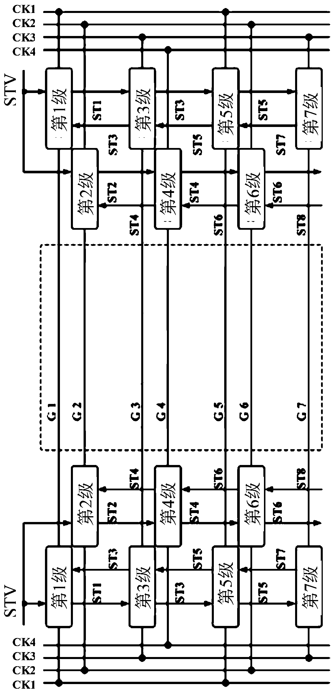
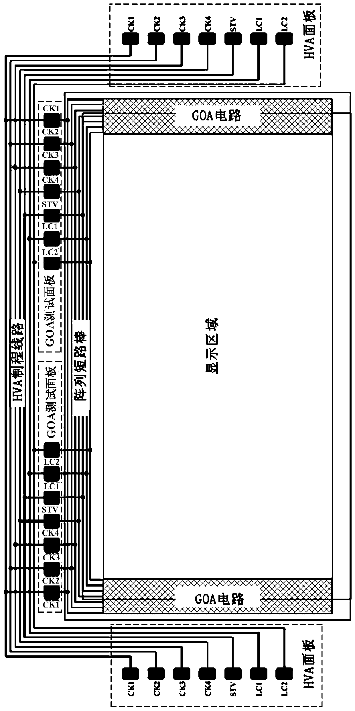
[0056] Figure 6 is the first embodiment of the present invention, and figure 2 The circuit design in is similar. Figure 6 The GOA test panels in the test are also all connected to the HVA process lines. but with figure 2 The difference is that in addition to the four clock signals in the peripheral circuit, the STV signal, LC1 signal and LC2 signal are all split according to the left and right sides. Specifically, the STV is split into the left STVL of the Q-point potential raising signal and the right STVR of the Q-point potential raising signal, which are used to provide STV signals to the GOA circuits on the left and right sides respectively. LC1 is split into a first pull-down circuit control signal left LC1L and a first pull-down circuit control signal right LC1R, which are used to provide LC1 signals to the left and right GOA circuits respectively. LC2 is split into a second pull-down circuit control signal left LC2L and a second pull-down circuit control signal ...
Embodiment 2
[0065] When using the liquid crystal panel test circuit provided in Embodiment 1 to carry out the GOA test process, it is only necessary to add different signals to the left and right GOA circuits through the left and right GOA test panels to realize the inspection of the GOA circuits on both sides.
[0066] For example, when checking the GOA circuit on the left, you can add a corresponding signal to the GOA circuit on the left through the GOA test panel on the left, and turn off the GOA circuit on the right. The signal waveform required at this time is as follows Figure 7 shown. From Figure 7 It can be seen that the four clock signals at this time are respectively related to Figure 4 The four clock signals in the same, STVL and Figure 4 The STV in the same, LC1L and LC2L are also with Figure 4 LC1 and LC2 in are the same. Four clock signals, STVL, LC1L and LC2L, can ensure the normal operation of the left GOA circuit. If a stage in the left GOA circuit fails, there w...
Embodiment 3
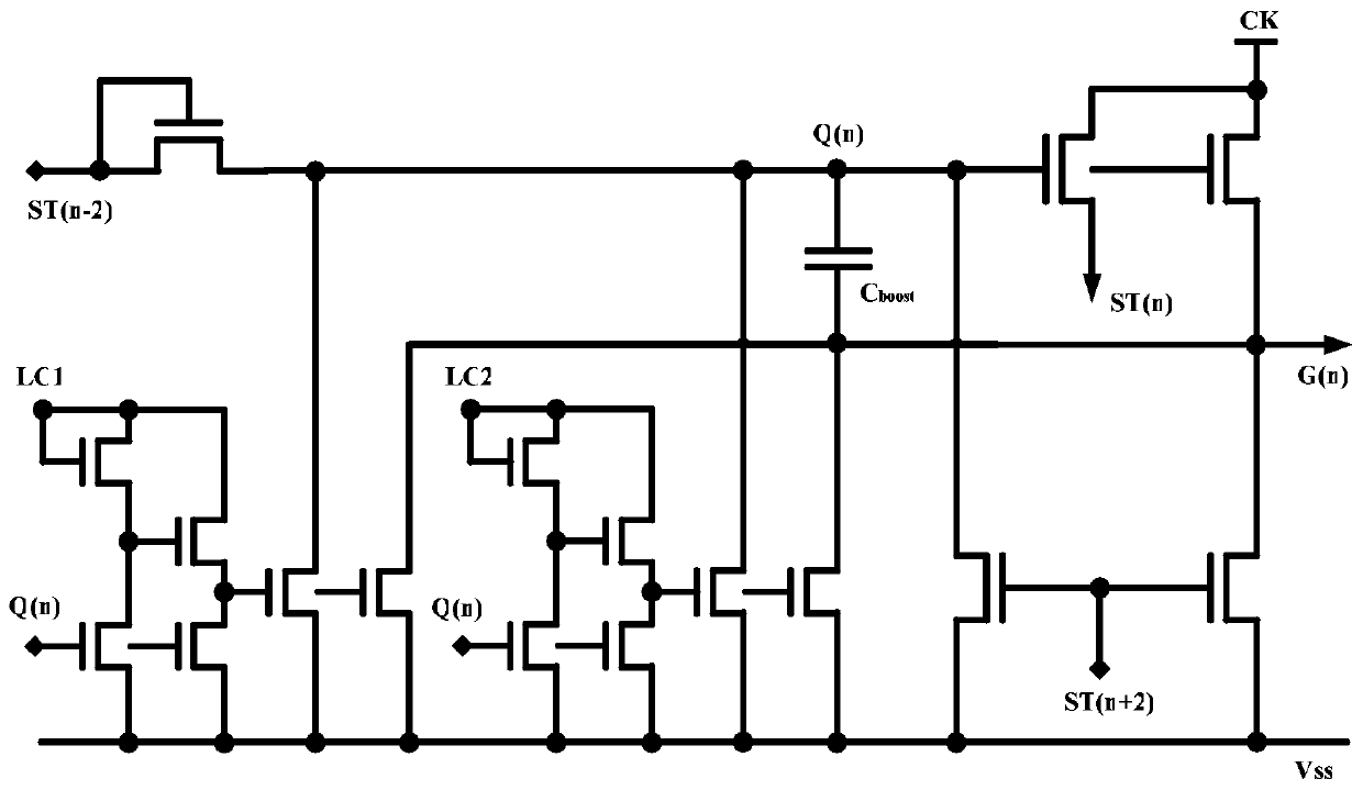
[0070] Such as Figure 9 As shown, this embodiment improves the GOA circuit. Figure 9 The GOA circuit shown with image 3 In contrast, a thin film transistor Tx is added in each level of GOA unit. Wherein, the gate of the thin film transistor Tx is used to receive the newly added reset signal, and the source and drain of the thin film transistor Tx are respectively connected to the gate line Gn and the low voltage signal Vss.
[0071] The peripheral circuit connection of the improved GOA circuit is connected with Figure 6 Exactly the same, STV, LC1, and LC2 are still divided into six signals: STVL / R, LC1L / R, and LC2L / R according to the left and right sides, and the four CK signals are shared on both sides, and the newly added reset signal Resst is also on both sides shared.
[0072] During the GOA test, Resst is a low-potential DC signal, and other signals are the same as Figure 7 same. In this way, the GOA circuits on the left and right sides can be inspected separat...
PUM
 Abstract
Description
Claims
Application Information
 - R&D Engineer
- R&D Manager
- IP Professional
- Industry Leading Data Capabilities
- Powerful AI technology
- Patent DNA Extraction
Browse by: Latest US Patents, China's latest patents, Technical Efficacy Thesaurus, Application Domain, Technology Topic, Popular Technical Reports.
© 2024 PatSnap. All rights reserved.Legal|Privacy policy|Modern Slavery Act Transparency Statement|Sitemap|About US| Contact US: help@patsnap.com