Light scanning device and image forming apparatus
An optical scanning device and deflection scanning technology, which is applied in the field of optical scanning devices and image forming devices, can solve the problems of reduced scanning accuracy of light beams, bending of the first imaging lens, and reduced optical performance of the first imaging lens, and achieve the goal of improving scanning accuracy Effect
- Summary
- Abstract
- Description
- Claims
- Application Information
AI Technical Summary
Problems solved by technology
Method used
Image

Examples
Embodiment approach 1
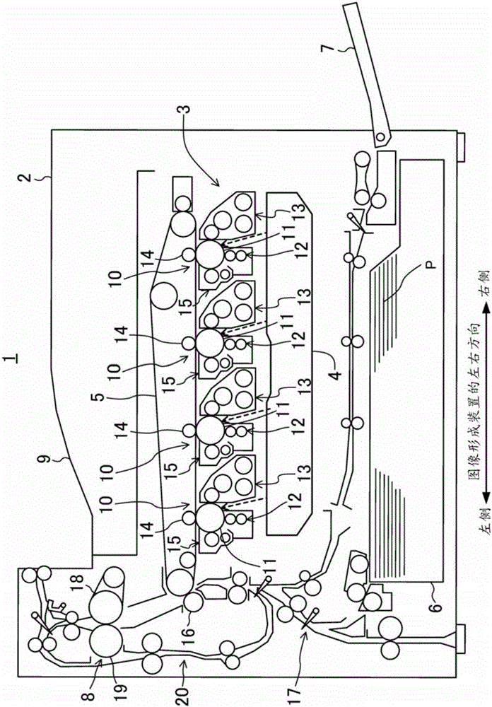
[0021] figure 1 It is a schematic configuration diagram showing the image forming apparatus 1 in the embodiment. The image forming apparatus 1 is a tandem color printer, and includes an image forming unit 3 inside a box-shaped casing 2 . The image forming unit 3 transfers and forms an image on the recording paper P based on image data transmitted from an external device such as a computer connected to a network or the like. Below the image forming unit 3 , an optical scanning device 4 for irradiating a beam (laser) is arranged, and above the image forming unit 3 , a transfer belt 5 is arranged. Below the optical scanning device 4 , a paper storage unit 6 for storing recording paper P is disposed, and a manual paper feed unit 7 is disposed on the side of the paper storage unit 6 . On the side upper portion of the transfer belt 5 , a fixing unit 8 for performing a fixing process on an image transferred and formed on the recording paper P is arranged. A mark 9 is a paper disch...
Embodiment approach 2
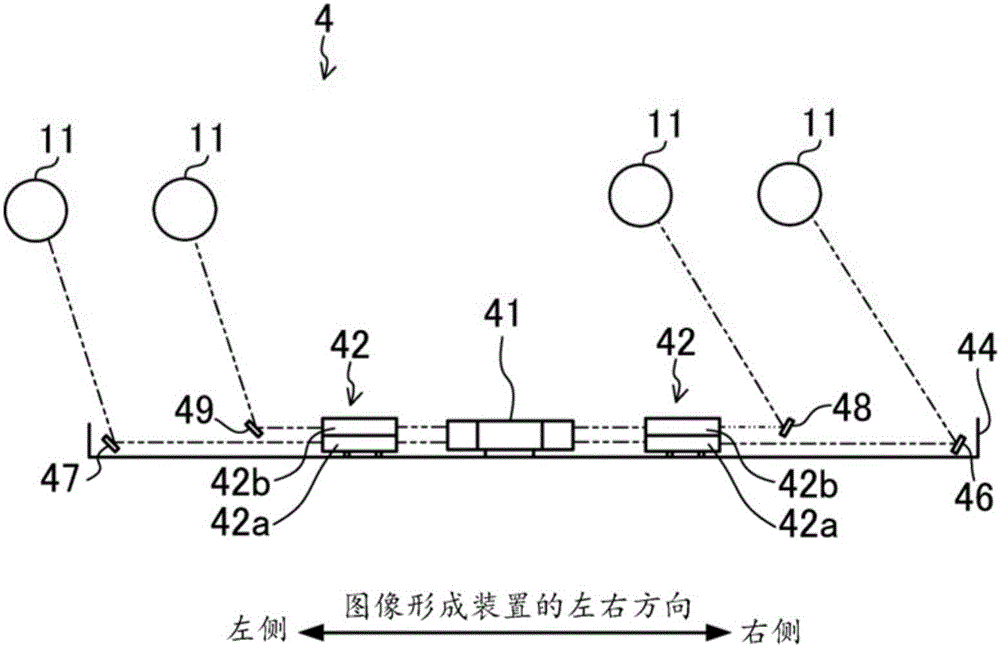
[0037] Figure 5 Embodiment 2 is shown. In this embodiment, the bonding area between each upper bonding portion 52 and the lower imaging lens 42 a is different from that in the first embodiment described above. In addition, except for this point, the structure of this embodiment is the same as that of Embodiment 1. In the following embodiments, the same components as those in the first embodiment are given the same symbols, and detailed description thereof will be omitted.
[0038] That is, in the present embodiment, the bonding area between each upper bonding portion 52 and the lower imaging lens 42a is set larger than the bonding area between each lower bonding portion 51 and the lower imaging lens 42a. Thereby, the adhesive force of the pair of upper adhesive parts 52 to the two imaging lenses 42a, 42b can be strengthened, thereby reliably suppressing the bending deformation of the lower imaging lens 42a caused by changes in ambient temperature. Therefore, the same effec...
Embodiment approach 3
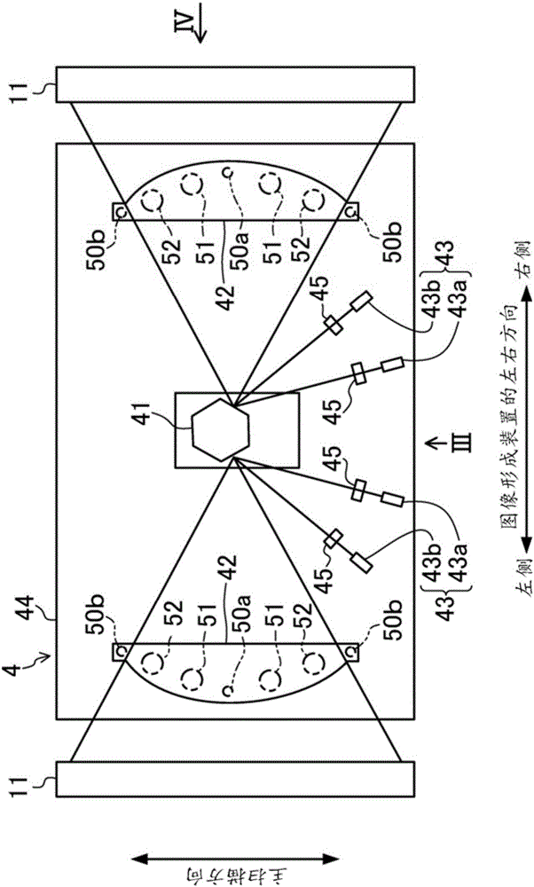
[0040] Figure 6 Embodiment 3 is shown. This embodiment differs from the above-described embodiments in that the lower adhesive portion 51 is more easily deformed in the main scanning direction than the upper adhesive portion 52 . In addition, except for this point, the structure of this embodiment is the same as that of Embodiment 1.
[0041] That is, in the present embodiment, the bonding area of each lower bonding portion 51 and the lower imaging lens 42a is equal to the bonding area of each upper bonding portion 52 and the lower imaging lens 42a, and the lower side The distance h2 between the imaging lens 42a and the bottom wall of the housing 44 is set to be sufficiently larger (for example, twice or more) than the distance h1 between the lower imaging lens 42a and the upper imaging lens 42b. Accordingly, the lower adhesive portion 51 is more easily deformed in the main scanning direction than the upper adhesive portion 52 . Therefore, when the ambient temperature ...
PUM
 Abstract
Description
Claims
Application Information
 - Generate Ideas
- Intellectual Property
- Life Sciences
- Materials
- Tech Scout
- Unparalleled Data Quality
- Higher Quality Content
- 60% Fewer Hallucinations
Browse by: Latest US Patents, China's latest patents, Technical Efficacy Thesaurus, Application Domain, Technology Topic, Popular Technical Reports.
© 2025 PatSnap. All rights reserved.Legal|Privacy policy|Modern Slavery Act Transparency Statement|Sitemap|About US| Contact US: help@patsnap.com