Wide-range optical delay device

A technology of optical delay and large range, applied in the direction of optical fiber transmission, etc., can solve the problems of inability to continuously adjust the optical path, complex structure, low precision, etc., to achieve continuous scanning function, flexible and diverse structure, and high scanning accuracy Effect

Active Publication Date: 2014-04-23
HARBIN ENG UNIV
View PDF7 Cites 14 Cited by
  • Summary
  • Abstract
  • Description
  • Claims
  • Application Information

AI Technical Summary

Problems solved by technology

At present, the commonly used variable optical delay line is composed of multiple optical fibers or optical waveguides, and the length of each optical path is different. Through the selection of cascaded optical switches, the optical signal can pass through optical fibers or waveguides of different lengths to obtain different delay times. , but for now, the optical delay line has several disadvantages: 1. The incrementally adjustable delay line has a large delay range, but it is not continuously adjustable; 2. The continuously adjustable delay line has high adjustment accuracy, but The delay range is usually small, usually below a few hundred ps; 3. The delay line connection loss is large and the accuracy is low
[0006] In 2007, people such as Oleg M.Efimov of the United States disclosed a kind of digitally controllable optical delay line [Digitally controlled optical fiber delay line, US Patent, 7283708B2], this invention has utilized the optical fiber module of multi-array (optical beam splitter , fiber amplifiers, connectors and optical collimators, etc.) to extend the optical path; compared with traditional methods, it is more powerful and versatile, but it cannot achieve continuous adjustment of the optical path, and the structure is more complicated

Method used


Image

  • Wide-range optical delay device
  • Wide-range optical delay device
  • Wide-range optical delay device

Examples


Embodiment 1

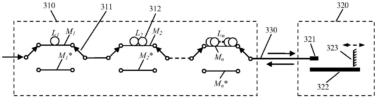
[0047] Example 1: Reflective large-range optical delay device

[0048] The structure of the delay device is as image 3 As shown, the selection of main optoelectronic devices and their parameters are as follows:

[0049] (1) The extension fiber is G.652 ordinary fiber 312, and the model is SMF28e;

[0050] (2) The working wavelength of the 2×2 optical switch 311 is 1550nm, and the insertion loss is ≤0.8dB;

[0051] (3) The working wavelength of the optical collimator 321 is 1550nm, the optical path scanning distance between it and the movable optical mirror 323 (the reflectivity is above 95%) is changed between 0-200mm, and the average insertion loss is 3.0dB;

[0052] (4) The central wavelength of the optical mirror 323 is 1550nm, the diameter is 20mm, the thickness is 2mm, the average reflectivity is >95%, the parallelism is 90%;

[0053] (5) The program-controlled translation stage 322 uses a 200mm translation platform with a position accuracy of 1 μm.

[0054] in such...

Embodiment 2

[0059] Example 2: Transmission-type large-range optical delay device based on double self-focusing lenses

[0060] Such as Figure 5 As shown, most of the photoelectric device parameters of the transmissive large-range optical delay device based on double self-focusing lenses are exactly the same as those in Example 1. The difference is that in Example 2, the 2×2 optical switch is replaced by 1×8 In the continuous optical path scanning device, a group of optical collimators, a group of optical mirrors and a program-controlled displacement stage are used together. The length of the periodic retarder is no longer multiplied, but two adjacent channels exist. For a fixed optical path difference, the specific device parameters are changed as follows:

[0061] (1) The working wavelength of 1×8 optical switch 511 is 1550nm, and the insertion loss is ≤0.8dB;

[0062] (2) The double optical collimators 521 and 522 and the double optical mirrors 523 and 524 are made of exactly the sam...

Embodiment 3

[0065] Embodiment 3: A transmission-type large-range optical delay device based on a three-port circulator

[0066] Such as Figure 6 As shown, most of the photoelectric device parameters of the transmission-type large-range optical delay device based on the three-port circulator are exactly the same as those in Embodiment 1 and Embodiment 2. The difference is that the device uses a three-port circulator in the continuous optical path In the scanning device, the specific parameters of the circulator are: the working wavelength is 1550nm, the insertion loss is 0.8dB, and the isolation is >50dB.

[0067] in such as Figure 6 In the shown structure, the same as in Embodiment 2, 1×8 optical switches are selected to form an 8-channel optical delay structure, and the optical path differences of the 8 channels are respectively 0cm, 13cm, 26cm, 39cm, 52cm, 65cm, 78cm, and 91cm; scanning The range of the stage is 0-200mm, and the position accuracy is 1 micron. Through calculation, i...


PUM


Abstract

The invention belongs to the field of optical fiber sensing and optical measured, in particular to a wide-range optical delay device. The wide-range optical delay device consists of a step type optical path multiplication device and a continuous optical path scanning device which are connected through a transmission optical fiber; wherein, the range of optical path continuous scanning of the continuous optical path scanning device is 0 to X0; the step type optical path multiplication device (110) is composed of n different delay light paths a0, a1 ...... an of fixed length, the optical path of delay light path is respectively L0, L1 ......, Ln (L0=0, n=0,1,2,......,), the optical path of adjacent delay light paths increases to meet Ln+1-Ln<X0, X0-d<Ln+1-Ln<X0, and Ln+2-Ln+1<=Ln+1-Ln, according to the invention, a fixed delay module and a variable optical path delay mechanism are combined together to achieve a continuous expansion of arbitrary optical path; the device realizes a seamless connection of the optical path by means of high-precision scanning platform to meet the continuous scanning function in the same precision.

Description

technical field [0001] The invention belongs to the field of optical fiber sensing and optical measurement, and in particular relates to a large-range optical delay device. Background technique [0002] In recent years, optical fiber transmission has been widely used and developed rapidly in the field of communication. The research and application of various optical fiber devices have also emerged. As a new signal processing device, the Fiber Delay Line (FDL) has developed from a simple section of optical fiber to an independent device with multiple complex structures at the present stage, and has become one of the key devices in optical information processing technology. Various signal processing functions, such as participating in the acquisition and transmission of measurement signals in optical fiber sensing and optical measurement systems, realizing signal encoding and buffering in optical fiber communication systems, and realizing accurate microwave signals in optical...

Claims


Application Information

Patent Timeline
Patent Type & Authority Applications(China)
IPC IPC(8): H04B10/25
Inventor 杨军柴俊苑勇贵彭峰吴冰苑立波
Owner HARBIN ENG UNIV
Why Eureka
Try Eureka