Touch substrate, manufacturing method thereof, and touch screen

A manufacturing method and touch screen technology, which can be used in programmable/customizable/modifiable circuits, instruments, electrical digital data processing, etc., can solve problems such as decreased insulation performance, decreased resistivity of black matrix patterns, etc., to avoid ESD , Improve the effect of anti-ESD ability

Active Publication Date: 2016-12-07
BOE TECH GRP CO LTD +1
View PDF5 Cites 10 Cited by
  • Summary
  • Abstract
  • Description
  • Claims
  • Application Information

AI Technical Summary

Problems solved by technology

[0004] Existing touch screens include a touch area for touch detection and a wiring area surrounding the touch area. In the wiring area, conductive wiring is made on a black matrix pattern. The black matrix pattern is generally made of carbon balls. Generally, the insulation performance of the black matrix pattern is better, but after multiple high-temperature processes, the resistivity of the black matrix pattern decreases, and the insulation performance decreases. In this way, if the distance between two adjacent conductive traces is relatively close in the trace area, Static electricity will be discharged through the black matrix pattern between these two conductive traces, resulting in ESD between the two conductive traces

Method used


Image

  • Touch substrate, manufacturing method thereof, and touch screen
  • Touch substrate, manufacturing method thereof, and touch screen
  • Touch substrate, manufacturing method thereof, and touch screen

Examples


Embodiment 1

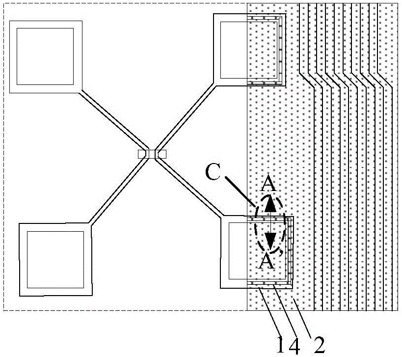
[0036] This embodiment provides a touch substrate, including a touch area on the base substrate 3 and a wiring area around the touch area, such as image 3 As shown, the wiring area includes: a black matrix pattern 2 covering the wiring area; a conductive wiring 1 located on the black matrix pattern 2, wherein two adjacent conductive wirings 1 located on the black matrix pattern 2 are arranged Conductive pattern 4 with ground.

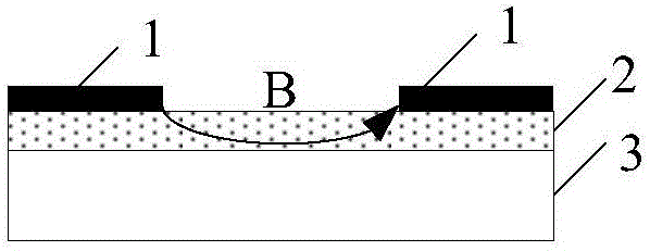
[0037] On the black matrix pattern, due to the decrease of the resistivity of the black matrix pattern, the ESD phenomenon is prone to occur between two adjacent conductive traces, so in this embodiment, the adjacent two conductive traces on the black matrix pattern There is a grounded conductive pattern between them, which can conduct away the static electricity between two adjacent conductive traces, thereby avoiding ESD between two adjacent conductive traces, thereby improving the ESD resistance of the touch substrate ability.

[0038] Preferably,...

Embodiment 2

[0044] like Figure 5 As shown, the present embodiment provides a touch screen, which includes the above-mentioned touch substrate, and further includes a protective structure 5 covering the touch substrate. The touch screen of this embodiment can be applied to human-computer interaction devices.

[0045] Further, the touch screen also includes a grounding point located outside the touch substrate, such as Figure 5 As shown, the protective structure 5 is provided with a via hole, and the conductive pattern 4 is electrically connected to a ground point outside the touch substrate through the via hole, so that the conductive pattern 4 can be grounded through the ground point.

[0046] Further, as Figure 5 As shown, the touch screen also includes:

[0047] The conductive lead 6 that runs through the via hole and connects the conductive pattern and the ground point, and the static electricity between adjacent conductive traces 1 is transferred to the ground point through the ...

Embodiment 3

[0050] This embodiment provides a method for manufacturing a touch substrate. The touch substrate includes a touch area and a wiring area surrounding the touch area. The manufacturing method includes forming a black matrix pattern in the wiring area and forming a black matrix pattern on the black matrix pattern. Conductive traces, such as Figure 4 As shown, the preparation method also includes:

[0051] A grounded conductive pattern 4 is formed between two adjacent conductive traces 1 .

[0052] On the black matrix pattern, due to the decrease of the resistivity of the black matrix pattern, the ESD phenomenon is prone to occur between two adjacent conductive traces, so in this embodiment, the adjacent two conductive traces on the black matrix pattern There is a grounded conductive pattern between them, which can conduct away the static electricity between two adjacent conductive traces, thereby avoiding ESD between two adjacent conductive traces, thereby improving the ESD re...


PUM


Abstract

The invention provides a touch substrate and a manufacturing method thereof, and belongs to the technical field of touch. The touch substrate comprises a touch area and a wiring area positioned around the touch area, wherein the wiring area comprises a black matrix pattern covering the wiring area, conductive routing wires positioned on the black matrix pattern, and a grounded conductive pattern arranged between the two adjacent conductive routing wires positioned on the black matrix pattern. According to the technical scheme provided by the invention, the anti-ESD ability of the touch screen can be improved.

Description

technical field [0001] The invention relates to the field of touch technology, in particular to a touch substrate, a manufacturing method thereof, and a touch screen. Background technique [0002] The touch panel is a device for positioning by calculating the coordinates of the touch points in the screen. The touch panel detects the user's touch position, then sends the detected information to the controller, converts it into coordinates, and sends To the central processing unit, at the same time accept the signal returned by the central processing unit and execute it to realize human-computer interaction. [0003] At present, most of the touch screens used in the market are capacitive touch screens, especially the new generation of touch devices represented by Apple mobile phones, which have greatly developed capacitive touch screens. The main application of capacitive touch screens is In products such as smartphones, tablets, and laptops. With the rapid growth of capacit...

Claims


Application Information

Patent Timeline
Patent Type & Authority Applications(China)
IPC IPC(8): G06F3/041
CPCG06F3/0412G06F3/0418G06F3/04164G06F2203/04103H05K1/0259H05K1/0289G06F3/044G06F2203/04107G06F2203/04111
Inventor 谢晓冬胡明张明何敏田健王庆浦
Owner BOE TECH GRP CO LTD
Why Eureka
Try Eureka