LED chip and preparation method thereof

An LED chip, N-type technology, applied in electrical components, electro-solid devices, circuits, etc., can solve problems such as threats and damage to electronic components, and achieve the effect of improving reliability and enhancing ESD resistance.

Inactive Publication Date: 2018-05-29
FOCUS LIGHTINGS SCI & TECH
View PDF4 Cites 2 Cited by
  • Summary
  • Abstract
  • Description
  • Claims
  • Application Information

AI Technical Summary

Problems solved by technology

[0002] ESD (Electro-Static discharge, electrostatic discharge) will pose a serious threat to electronic components such as LED chips. The most common cause of ESD is friction between two different substances

Method used


Image

  • LED chip and preparation method thereof
  • LED chip and preparation method thereof
  • LED chip and preparation method thereof

Examples


Example Embodiment

[0037] The present invention will be described in detail below in conjunction with the specific embodiments shown in the drawings. However, these embodiments do not limit the present invention, and the structural, method, or functional changes made by those skilled in the art based on these embodiments are all included in the protection scope of the present invention.

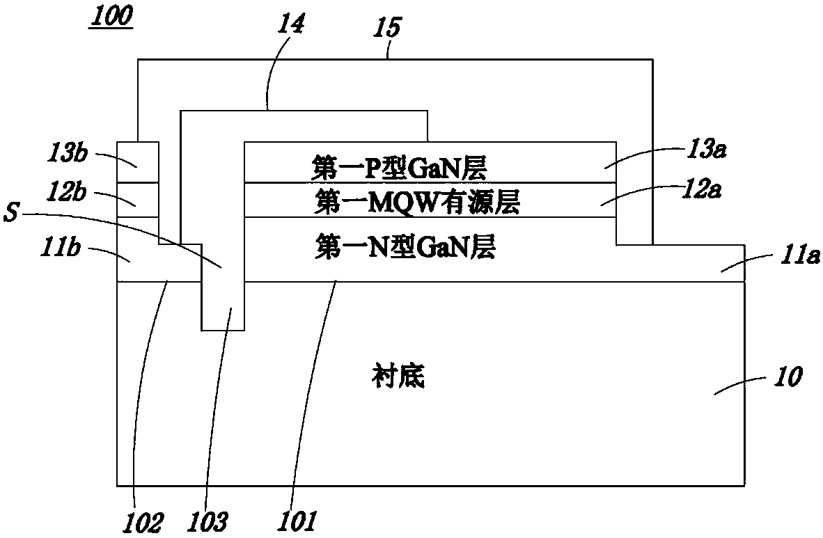
[0038] Such as figure 1 Shown is a schematic diagram of an LED chip according to an embodiment of the present invention.

[0039] The LED chip 100 includes a substrate 10, and the substrate 10 includes a middle area 101 and an edge area 102.

[0040] The intermediate region 101 includes a first N-type GaN layer 11a, a first MQW active layer 12a, and a first P-type GaN layer 13a in order from bottom to top.

[0041] The edge region 102 sequentially includes a second N-type GaN layer 11b, a second MQW active layer 12b, and a second P-type GaN layer 13b from bottom to top.

[0042] Among them, the first P-type GaN layer 13...


PUM


Abstract

The invention discloses an LED chip and a preparation method thereof. The LED chip includes a substrate. The substrate includes a middle region and an edge region. The middle region includes a first N-type GaN layer, a first MQW active layer and a first p-type GaN layer in sequence from bottom to top. The edge region includes a second n-type GaN layer, a second MQW active layer, and a second p-type GaN layer in sequence from bottom to top. The first p-type GaN layer is connected with the second n-type GaN layer. The first N-type GaN layer is connected with the second P-type GaN layer. In the invention, the edge portion of the LED chip with poor light emission distribution is independently formed into a micro-diode, the micro-diode forms an anti-parallel structure with the original chip, inthis way, the anti-ESD capability of the LED chip is enhanced and the reliability of the LED chip is improved.

Description

technical field [0001] The invention relates to the technical field of semiconductor light emitting devices, in particular to an LED chip and a preparation method thereof. Background technique [0002] ESD (Electro-Static discharge, electrostatic discharge) will pose a serious threat to electronic components such as LED chips. The most common cause of ESD is friction between two different substances, causing charges to accumulate on their surfaces and accumulate energy. , these accumulated energies are released in the form of current surges or voltage transients, causing damage to electronic components. [0003] The easiest way to achieve effective ESD protection is grounding, which provides a low-impedance current path to ground, but electronic components will inevitably suffer from ESD interference during transportation and use. How to enhance the anti-ESD ability of electronic components such as LED chips becomes particularly important. Contents of the invention [00...

Claims


Application Information

Patent Timeline
IPC IPC(8): H01L23/60H01L25/16H01L33/06H01L33/00
CPCH01L25/167H01L23/60H01L33/007H01L33/06
Inventor 李庆陈立人余长治
Owner FOCUS LIGHTINGS SCI & TECH
Why Eureka
Try Eureka